印刷电路板制造
将您的愿景变为现实:利用 Bester 释放定制 PCB 制作的力量!
印刷电路板制造
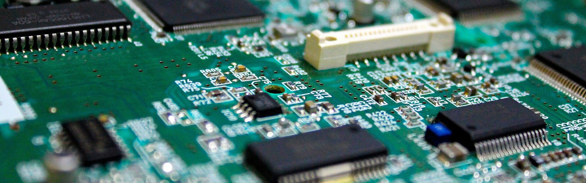
电路板制造是电子设备制造过程中的一个关键步骤。它涉及创建一个定制设计的电路板,作为各种电子元件的基础。这一过程始于设计阶段,在这一阶段要确定电路板的布局和规格。设计完成后,将其转印到覆铜层压材料上,作为电路板的基底。下一步是蚀刻掉多余的铜,留下所需的电路图案。这是通过化学蚀刻和光刻技术的结合来实现的。蚀刻过程结束后,要对电路板进行彻底清洁,以去除任何残留物和污染物。下一个关键步骤是钻孔,钻孔是为了放置元件和进行电气连接。然后对这些孔进行电镀,以确保安全连接。钻孔和电镀完成后,就会使用阻焊层来保护电路并提供绝缘。最后是丝印层,包括元件标签、标识和其他识别标记。电路板制作要求精确和专业,以确保电路板的最高质量和功能。

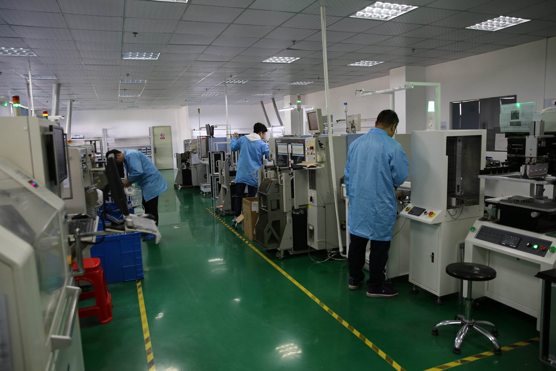
在 Bester,我们很荣幸能为尊贵的客户提供一流的印刷电路板制作服务。凭借在该领域多年的经验和专业知识,我们致力于提供符合客户独特要求和规格的高质量印刷电路板。我们先进的生产设施配备了先进的技术和尖端的机械设备,使我们能够精确无误地生产印刷电路板。我们拥有一支技术娴熟的工程师和技术人员团队,他们兢兢业业,确保从最初设计到最终生产的每一个制造环节都得到精心执行。我们非常注重质量控制,实施严格的测试程序,以保证我们制造的每块印刷电路板的可靠性和功能性。无论是小规模项目还是大规模生产,我们都有能力处理任何规模的订单。
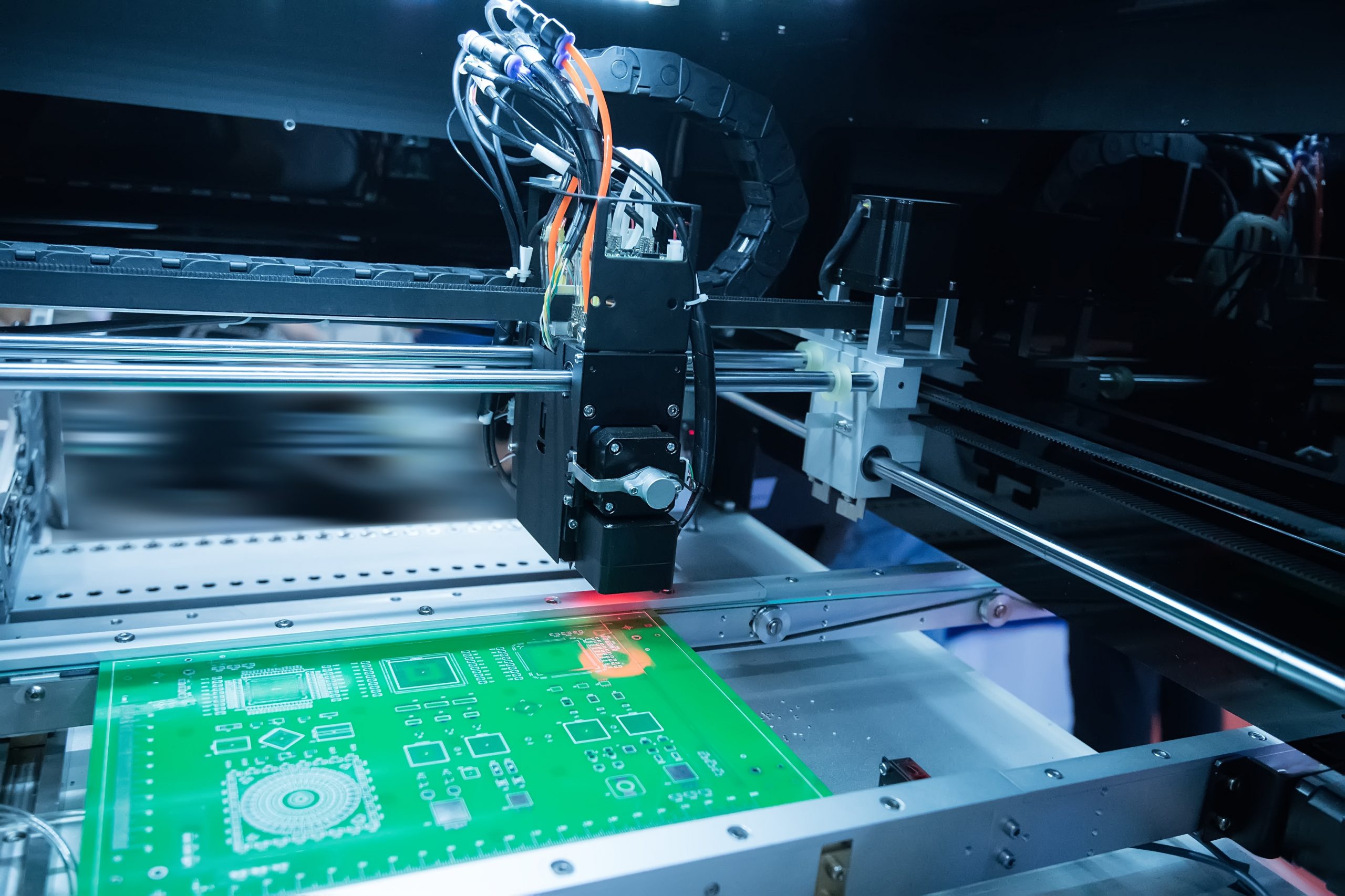
印刷电路板制造工艺
没有所谓的标准印刷电路板。每块印刷电路板对于特定产品都有独特的功能。因此,生产印刷电路板是一个由许多步骤组成的复杂过程。本概述涵盖了生产多层印刷电路板时最重要的步骤。当您从 Bester Tech 订购 PCB 时,您购买的是长期投资的优质产品。Bester Tech 的产品规格和质量控制比其他供应商严格得多,从而保证了产品质量。在下面的生产流程中,您可以看到该流程的独特之处或超出 IPC 标准的地方。
生产前
我们使用您提供的数据(Gerber 文件)为您的定制电路板创建生产信息。我们的专家会将您的规格与产能相匹配,以符合要求。
内层成像
在制作电路板时,成像过程是电路轨迹的定义过程。传统的成像工艺需要紫外光和照相工具来传输图像,而 LDI 只使用计算机控制的高度集中的激光束,直接在电路板上确定电路图案。
内层蚀刻
利用蚀刻工艺消除面板上任何不良的铜残留物。除去干膜后,我们还会保留铜电路,这与印刷电路板的设计是一致的。
内层 AOI
根据数字图像检查电路,以验证电路是否与设计相符,是否存在缺陷。通过对电路板进行扫描,然后由训练有素的检验员对扫描过程中发现的任何异常进行验证。
层压
在电路板内层涂上氧化层,然后使用预浸料将它们堆叠在一起,在它们之间形成绝缘层。 上层和下层堆叠部分都要添加铜箔。
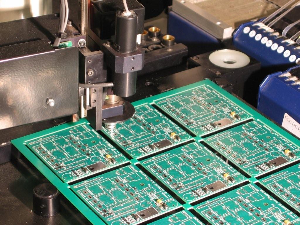
PCB 钻孔
钻孔,这些孔日后将作为多层电路板上的电气触点。钻孔是一个机械过程,PCB 制造商会对其进行优化,以获得内部层链接的注册。
化学沉铜
在墙壁上先前钻好的孔上涂上薄薄的铜层。PTH 提供的铜沉积层可掩盖孔壁和整个面板。
外层成像
外层成像类似于内部分层工艺。不过,在外层钻孔时,应去除干膜并保留电路。然后在干净的环境中镀上多余的铜。
图形电镀
第二种电解电镀工艺,我们在干膜部件(电路)上进行额外电镀。镀铜后,我们应该涂上锡,以防止镀铜氧化。
外层蚀刻
取出干燥的蓝色薄膜,刮除所有不需要的铜残留物。锡沉积物会抵制蚀刻过程,以保护铜沉积物,然后用化学方法消除锡残留物,留下电路。
焊接掩模
在艺术品和紫外线的帮助下,暴露 PCB 的一些部件,并移除所有暴露的部件。然后完全固化剩余的阻焊层,以获得高质量的表面效果。
表面处理
表面处理可以保持裸露的铜电路,同时在将元件焊接到印刷电路板时提供可焊表面。金属表面处理和有机表面处理是两种主要的表面处理方式。
电气测试
在发货前对所有电路板进行测试,以确保所有印刷电路板无缺陷并符合您所期望的标准。测试包括飞针、无夹具测试仪。我们还具备通用栅格测试能力。这些设备使用专为印刷电路板制造的夹具。
剖析
根据生产文件将印刷电路板生产面板加工成特定的尺寸和形状。PCB V 形刻线是在印刷电路板的顶部和底部切割出一个 "V "形槽,在 V 形槽之间留下薄薄的一层。完成后,只需施加极小的压力,就能在 V 形槽处轻松分离印刷电路板。
最终目视检查
一组目光敏锐的人员会仔细检查每件产品。这个过程包括按照既定标准目测电路板。
快速 PCB 原型开发和小批量生产
我们的印刷电路板组装能力包括但不限于下面列出的内容,因为我们会不断更新设备,使我们始终处于最前沿。
- 电路板规格
- 最大面板尺寸:19.7 英寸 x 31.5 英寸,最大层数:1-40,铜厚:0.5 盎司至 5.0 盎司,最小线宽:3 密耳,最小线间距:3 密耳,最小孔:0.006 英寸,盲孔、埋孔和插孔,受控阻抗:3 mil,最小孔:0.006″,盲孔、埋孔和塞孔,受控阻抗
- 材料
- 厚度:0.008 英寸至 0.240 英寸,FR-4、高 TG FR-4、聚四氟乙烯、铝基、罗杰斯,根据您的要求提供特殊材料
- 焊接掩模
- LPI - 绿、黄、黑、红、蓝、白等(询问更多选项),可剥离掩膜
- 最终完成
- SMOBC (HASL)、碳、选择性镀金、硬金和软金、沉金、沉银、沉锡、OSP
- 图例
- 白色、黄色、黑色(如需更多选择,请咨询)
- 检查方法
- 100% 外观检查、电气测试 - 飞针或钉床、样品批量检查、横截面检测
- 送货
- 急件:24 小时,标准原型:5 天,标准生产:10 天
为什么选择 Bester

强大的装配能力
我们拥有最先进的设施和技术精湛的团队,有能力处理最复杂的 PCB 组装项目,确保高效、准确地制造您的产品。

质量保证
我们严格的质量控制流程和广泛的测试程序确保我们生产的每个 PCB 组件都符合可靠性和性能方面的最高行业标准,让您对我们的服务放心和充满信心。

一站式服务
从 PCB 制作和设计到元件采购和 IC 编程,Bester 在同一屋檐下为您提供全面的服务,简化生产流程,节省您的时间和精力。

快速周转
我们对快速周转时间的承诺意味着您的印刷电路板组装项目将如期完成,使您能够在截止日期前完成生产,并迅速将产品推向市场。
客户和认证

Bester 的电子制造能力
制造能力
- 100% ESD 元件控制装置
- 8 条 SMT 线
- 4 个 DIP 线路
- 40 自动机器人焊接
- 数控加工
- 自动保形涂料
- 注塑成型
- 三维打印
认证
- ISO 9001
- UL
- SGS
- IPC
- RoHS
- CE
- 联邦电信交通委员会
- SRDI(中国 "专精特新 "企业)
- HNTE(中国高新技术企业)
我们服务的行业

汽车
我们深知 PCBA 在汽车行业中的关键作用。我们提供全面的 PCBA 服务,满足汽车制造商的特定需求,帮助他们提供可靠、高性能的电子系统。
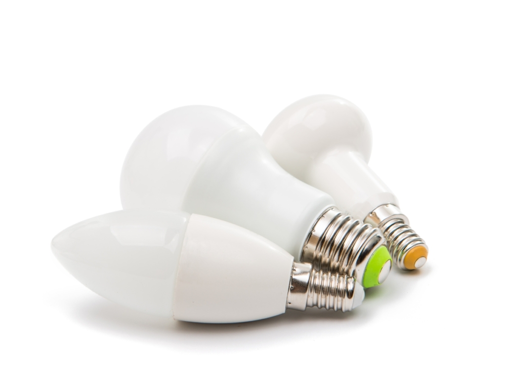
发光二极管
在 LED 市场,Bester 提供一流的 PCBA 解决方案,这对生产高质量的 LED 照明产品至关重要。我们与 LED 制造商密切合作,确保他们的 PCBA 符合能效、耐用性和性能方面的严格要求。
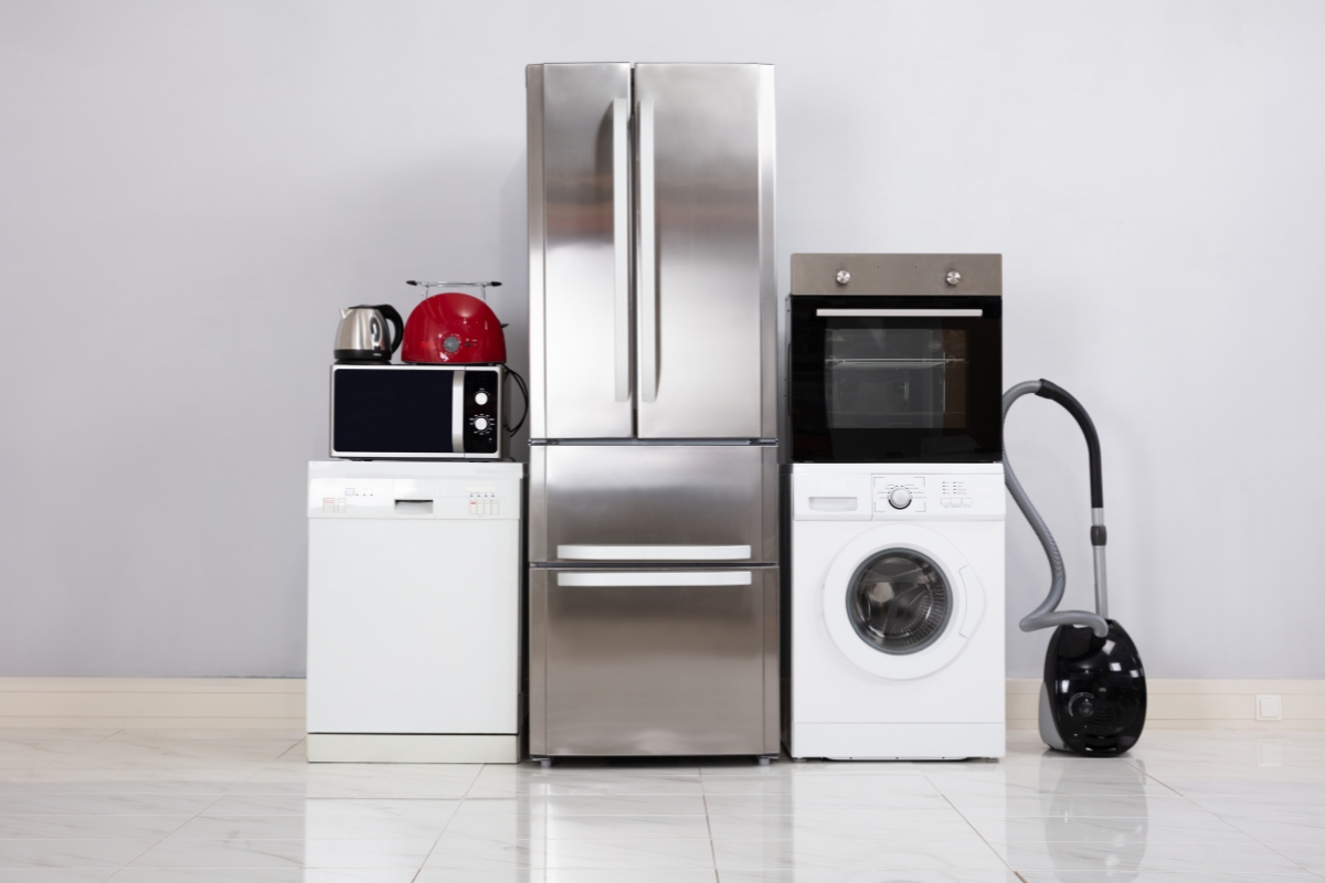
消费电子产品
Bester 通过提供广泛的 PCBA 服务来满足消费电子市场的需求,从而生产出创新的、用户友好的电子设备。我们与消费电子产品制造商合作,确保他们的 PCBA 符合最高的质量和功能标准。

工业
在工业领域,Bester 的 PCBA 服务在开发可靠、高效的电子系统方面发挥着至关重要的作用。我们与工业设备制造商密切合作,以满足他们的特定要求,确保我们的 PCBA 能够承受恶劣的环境条件,并提供最佳性能。
pcba 应用
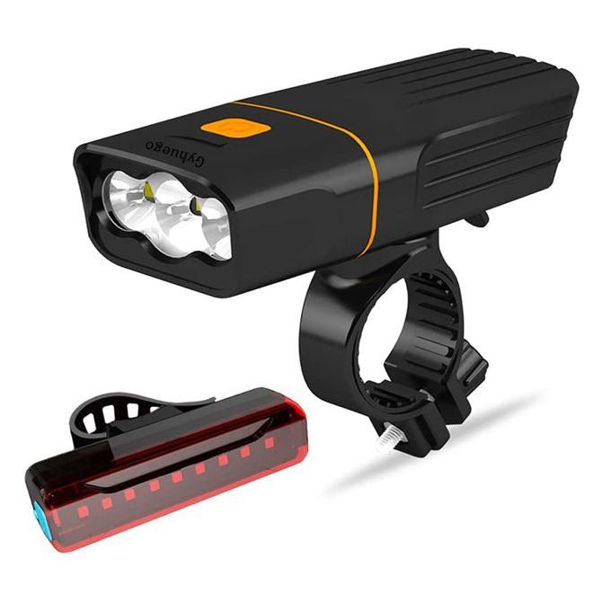
自行车灯 PCBA
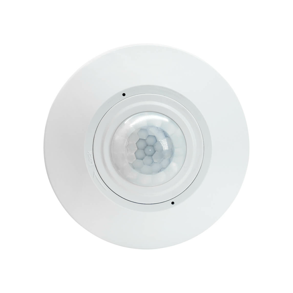
PIR 移动传感器 PCBA
LED PCBA
印刷电路板制造常见问题
如何获得标准印刷电路板的报价
只需点击或拨打一个电话,即可获得免费的 PCB 报价。请给我们发送电子邮件或致电,以获得最快速的报价。
使用 Bester 制作 PCB 的优势
Bester 是一个提供全方位服务的交钥匙 PCB 解决方案,可以处理从原型到制造再到组装的所有工作。十多年来,我们一直在制造高质量的标准 PCB,并完全符合 ISO9001:2015 质量标准。我们的所有标准印刷电路板均符合 IPC2 标准,并进行严格的内部质量保证测试,以确保运抵您工厂的电路板值得信赖。
我们提供符合您预算的 PCB 解决方案。您可以订购几块原型板来测试您的设计,然后批量订购标准印刷电路板,以节省更多费用。我们将为您提供免费的即时报价,让您了解自己的期望值,从而制定相应的计划。我们还提供来自 PCB 专家的全面技术支持。如有任何问题,请致电我们、在线聊天或发送电子邮件给我们,无论哪种方式对您来说最方便。我们会尽快处理您的疑虑或问题。我们已获得 99% 以上的客户满意度,只要您开始订购印刷电路板,我们就会立即为您提供服务。

准备好开始您的 PCB 组装项目了吗?