PCB 设计
利用我们尖端的 PCB 设计服务释放创新潜能
PCB 设计
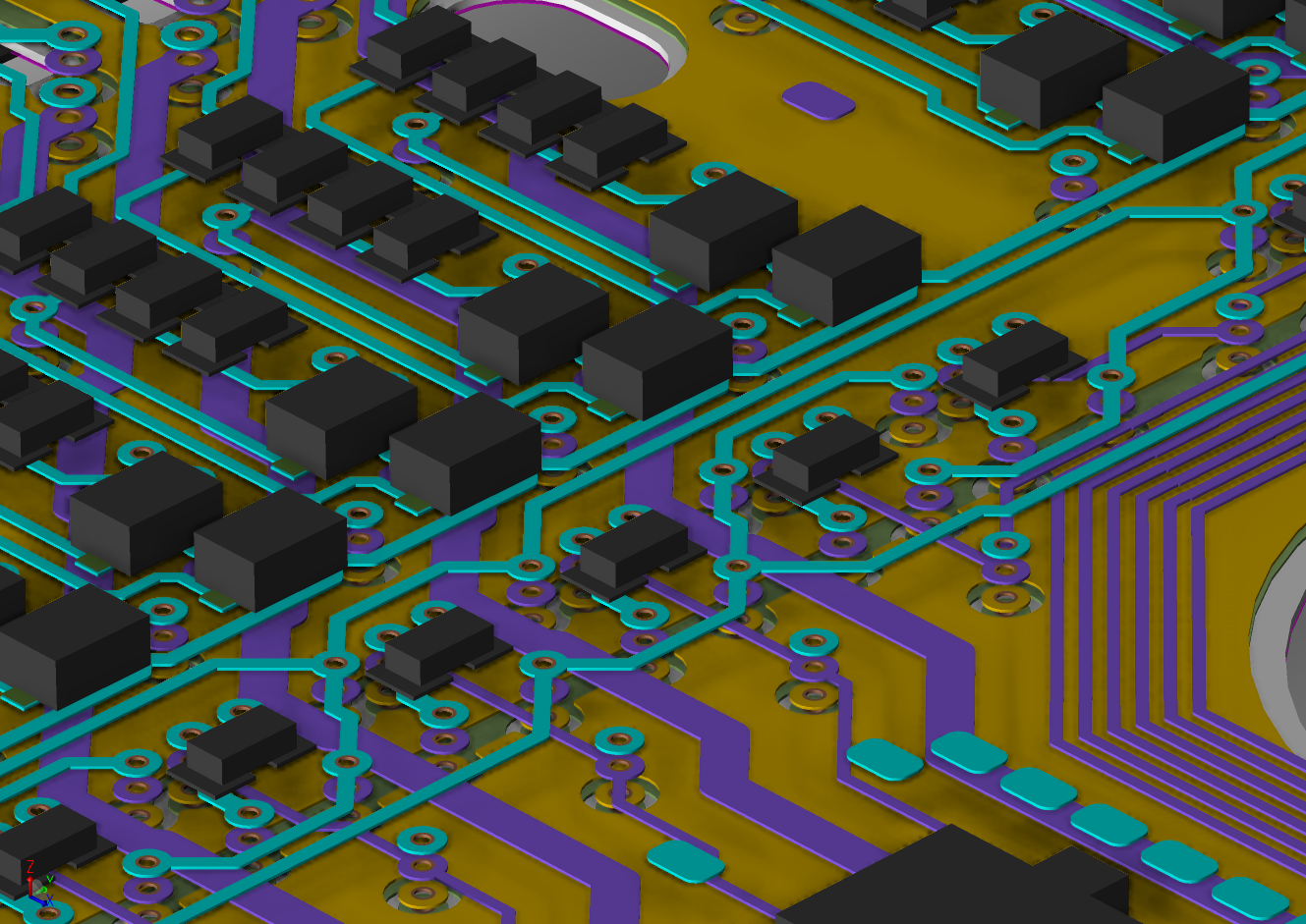
印刷电路板设计是在印刷电路板上创建电子元件布局和排列的过程。制造过程中的这一关键步骤包括将电路原理图转化为可制造和组装的物理设计。我们的团队由技术娴熟、经验丰富的设计师组成,利用最新的设计软件和工具,确保 PCB 设计准确高效。我们注重细节,注重功能,力求设计出性能、可靠性和可制造性均达到最佳的 PCB 设计。无论您需要的是简单的单层设计还是复杂的多层设计,我们都能提供满足您特定要求的高质量 PCB 设计。

Bester 为我们尊贵的客户提供一流的 PCB 设计服务,并引以为豪。我们拥有一支技术精湛、经验丰富的设计师团队,确保每个项目都经过精心设计,以满足客户的独特要求和规格。我们拥有尖端的设计软件和先进的技术,能够创造出高效、创新的 PCB 设计,并对性能、可靠性和成本效益进行优化。在整个设计过程中,我们与客户密切合作,不断提供沟通和反馈,以确保超越客户的期望。无论是复杂的多层设计还是简单的单层电路板,我们都拥有丰富的专业知识和资源,能够提供符合最高行业标准的卓越 PCB 设计解决方案。请相信 Bester 能满足您所有的 PCB 设计需求,体验与众不同的卓越品质。
PCB 设计服务能力
原理图捕捉
我们可以根据规格书、标注的原理图表或黑图和口头讨论创建原理图。我们接受任何格式的原理图(PDF、草图等),并可将其转换为首选的 CAD 格式。作为流程的一部分,我们会验证 BOM。
逆向工程
我们可以从裸板、组装板、现有设计文件和图纸中提取现有电路板。我们还可以创建一个带有所有支持文件的新设计。
成本优化
我们可以审查现有产品或设计,并提出降低成本的方法。在许多情况下,可以通过使用更小几何形状的导体和通孔以及激光钻孔微孔来减少层数。
PCB 叠加设计
在开始布局设计之前,我们将进行内部堆叠设计,以满足所有设计目标。我们还将建议是否需要采用 HDI 技术或帮助优化 PCB。
PCB 设计工具
我们使用 Cadence、Mentor Graphics 和 Altium 的标准工具。我们可以接受网表或部分/完全放置网表。我们可以使用我们的零件库或客户库。我们可以提供全天候服务,我们的设计团队可安排视频会议为您提供支持。我们可以利用离岸资源,在您睡觉时为您进行设计。
信号完整性服务
我们可以为任何高速电路板设计提供信号完整性服务。我们将满足控制阻抗和串扰要求;我们将提供适合实现特定信号完整性规范的印刷电路板材料。
PCB 设计能力
作为一家专业的印刷电路板和组装制造商,我们比其他供应商更了解如何设计可制造、可靠且经济高效的印刷电路板。
在 Bester Tech,您可以享受从 PCB 设计、PCB 制造到成品原型和大批量 PCB 组装设备的一站式 PCB 解决方案服务。我们成熟的工程方法可确保高效、经济的设计,并在第一时间完成。
我们提供两个阶段的设计审查,可以是离线审查,也可以是在线互动审查。可以使用行业标准的 PCB 设计软件提供 PCB 设计:
- 设计软件
-
- PADS (Mentor Graphics)
- Cadence(ORCAD 和 Allegro)
- Altium Designer (Altium)
- 提供的服务
-
- 我们可以接受任何形式的原理图(PDF、草图等),并将其转换为电子正确的 CAD 格式。
- 在原理图层面传达设计规则。
- 定制占地面积设计,满足您的需求。
- 对每种设计的 BOM 和部件价格进行竞争。
- 制作图纸、装配和 Gerber 文件,以满足制造要求。
- 刚性/柔性印刷电路板;可制作复杂的电路板形状。
- 交付产品
-
- 完整的原理图
- PCB 层堆叠图。
- 完整的 3D PDF 文件
- 制造文件(标准格式为 Gerber Extended;Gerber X2、ODB++、IPC-2581 可根据要求提供)
- 路由和钻孔文件
- 装配图
- 取放文件(中心点数据)
- 制造规格(层堆、钻孔表和图纸等)
- 完整的物料清单(BOM)
- 客户指定的其他输出
为什么选择 Bester

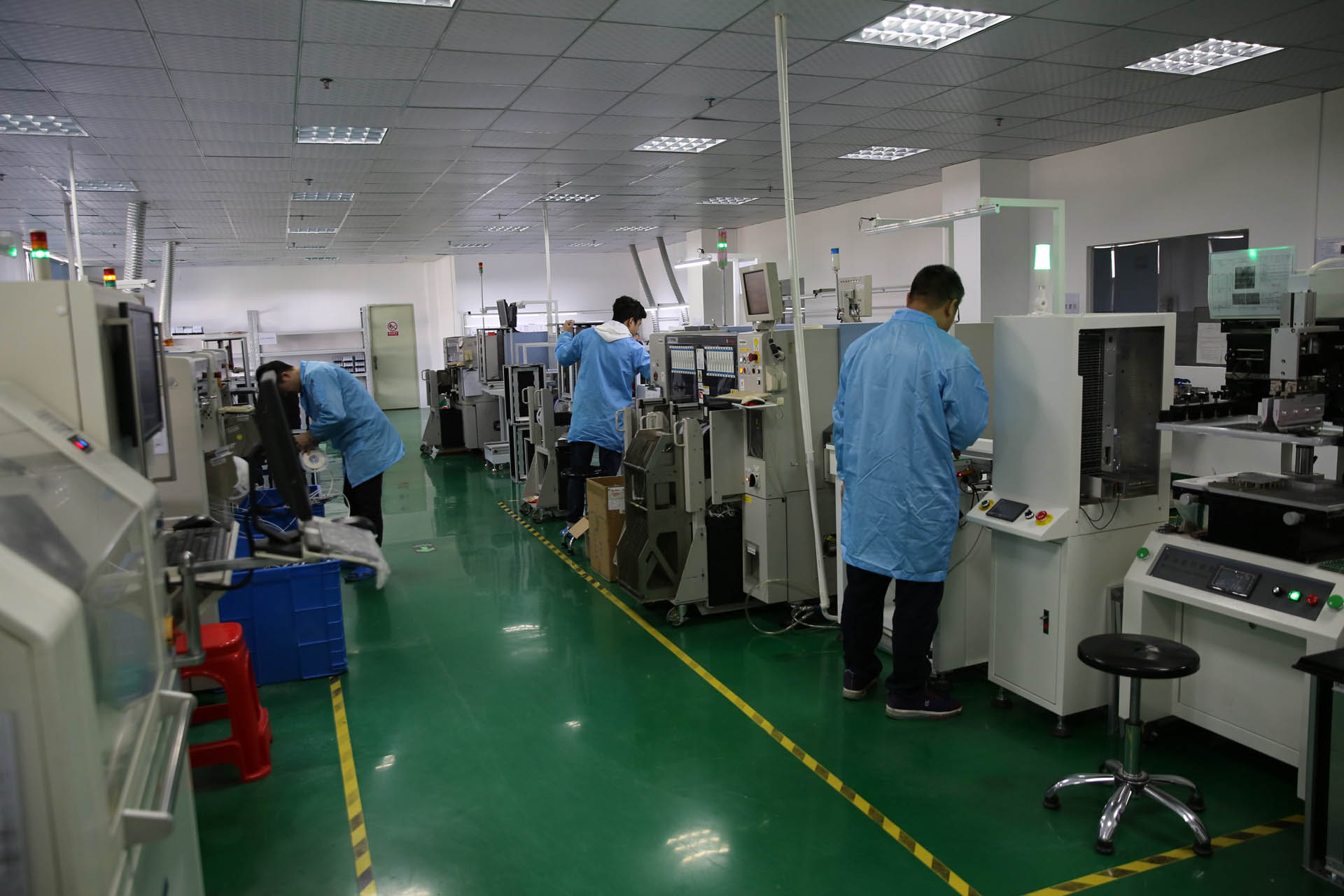
强大的装配能力
我们拥有最先进的设施和技术精湛的团队,有能力处理最复杂的 PCB 组装项目,确保高效、准确地制造您的产品。

质量保证
我们严格的质量控制流程和广泛的测试程序确保我们生产的每个 PCB 组件都符合可靠性和性能方面的最高行业标准,让您对我们的服务放心和充满信心。

一站式服务
从 PCB 制作和设计到元件采购和 IC 编程,Bester 在同一屋檐下为您提供全面的服务,简化生产流程,节省您的时间和精力。

快速周转
我们对快速周转时间的承诺意味着您的印刷电路板组装项目将如期完成,使您能够在截止日期前完成生产,并迅速将产品推向市场。
客户和认证

Bester 的电子制造能力
制造能力
- 100% ESD 元件控制装置
- 8 条 SMT 线
- 4 个 DIP 线路
- 40 自动机器人焊接
- 数控加工
- 自动保形涂料
- 注塑成型
- 三维打印
认证
- ISO 9001
- UL
- SGS
- IPC
- RoHS
- CE
- 联邦电信交通委员会
- SRDI(中国 "专精特新 "企业)
- HNTE(中国高新技术企业)
我们服务的行业

汽车
我们深知 PCBA 在汽车行业中的关键作用。我们提供全面的 PCBA 服务,满足汽车制造商的特定需求,帮助他们提供可靠、高性能的电子系统。
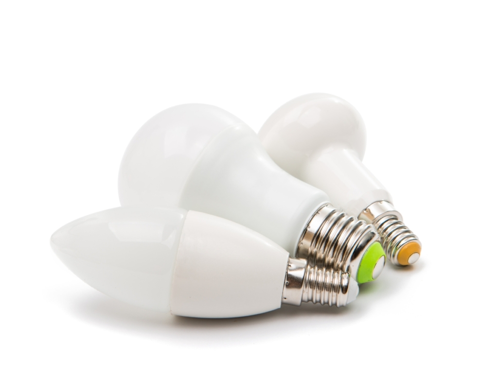
发光二极管
在 LED 市场,Bester 提供一流的 PCBA 解决方案,这对生产高质量的 LED 照明产品至关重要。我们与 LED 制造商密切合作,确保他们的 PCBA 符合能效、耐用性和性能方面的严格要求。
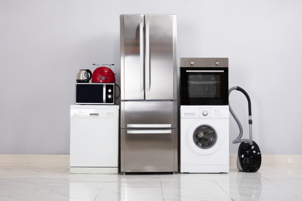
消费电子产品
Bester 通过提供广泛的 PCBA 服务来满足消费电子市场的需求,从而生产出创新的、用户友好的电子设备。我们与消费电子产品制造商合作,确保他们的 PCBA 符合最高的质量和功能标准。

工业
在工业领域,Bester 的 PCBA 服务在开发可靠、高效的电子系统方面发挥着至关重要的作用。我们与工业设备制造商密切合作,以满足他们的特定要求,确保我们的 PCBA 能够承受恶劣的环境条件,并提供最佳性能。
pcba 应用
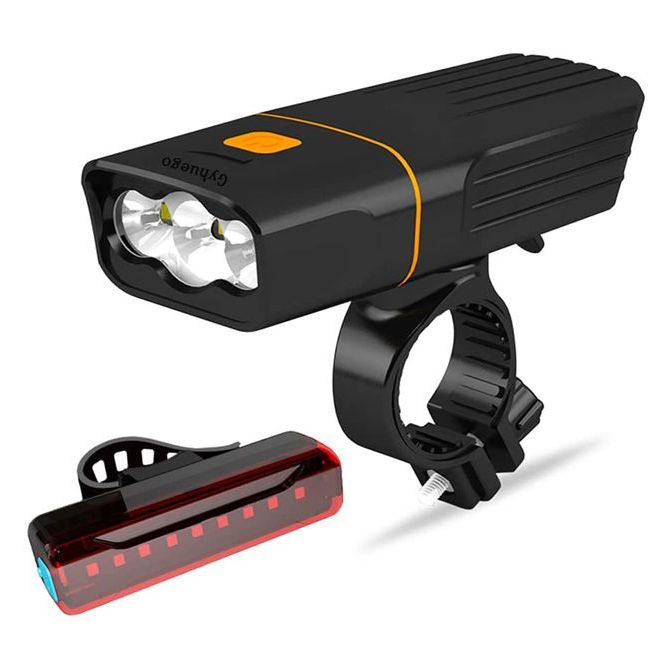
自行车灯 PCBA
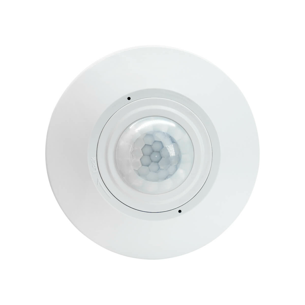
PIR 移动传感器 PCBA
LED PCBA
PCB 组装常见问题
您是经过认证的 PCB 制造商吗?
增材制造工艺又称快速成型制造工艺,是指利用加热打印头或激光等123444412312321 装置将各层材料结合在一起。这就是三维模型的精确复制品。
您是经过认证的 PCB 制造商吗?
增材制造工艺又称快速成型制造,是指使用三维打印机根据三维模型创建实体对象。该工艺需要逐层添加材料或长丝,然后使用粘合应用(如加热打印头或激光)将各层粘合在一起。最终得到的三维打印物体是原始三维模型的精确复制品。
您是经过认证的 PCB 制造商吗?
增材制造工艺又称添加式制造,是指使用三维打印机根据三维模型创建实体对象。该工艺需要逐层添加材料或长丝,然后使用熔融应用(如加热打印头或激光)将各层粘合在一起。最终得到的三维打印物体是原始三维模型的精确复制品。
你们提供快速 PCBA 服务吗?
快速成型材料工艺,也称为快速成型制造,是指使用三维打印机根据三维模型创建实体对象。该工艺需要逐层添加材料或长丝,然后使用熔融应用软件将材料熔化。
你们接受小批量订单吗?
增材制造工艺,又称增材制造,是指使用三维打印机根据三维模型创建实体对象。这一过程需要逐层添加材料或长丝,然后使用熔融应用(如加热打印头或激光)将各层粘合在一起。最终得到的三维打印物体是原始三维模型的精确复制品。

准备好开始您的 PCB 组装项目了吗?