印刷电路板制造
Transforming Your Vision into Reality: Unleash the Power of Customized PCB Fabrication with Bester!
PCB Fabrication
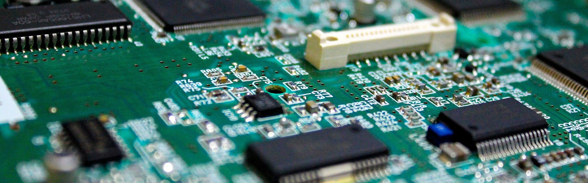
PCB fabrication is a crucial step in the manufacturing process of electronic devices. It involves the creation of a custom-designed circuit board that serves as the foundation for various electronic components. The process begins with the design phase, where the layout and specifications of the circuit board are determined. Once the design is finalized, it is transferred onto a copper-clad laminate material, which acts as the base for the PCB. The next step is to etch away the excess copper, leaving behind the desired circuitry pattern. This is achieved through a combination of chemical etching and photoengraving techniques. After the etching process, the board undergoes a thorough cleaning to remove any leftover residue and contaminants. The next crucial step is drilling, where holes are created for component placement and electrical connections. The holes are then plated to ensure a secure connection. Once the drilling and plating are complete, a solder mask is applied to protect the circuitry and provide insulation. Finally, a silkscreen layer is added, which includes component labels, logos, and other identification markings. PCB fabrication requires precision and expertise to ensure the highest quality and functionality of the circuit board.

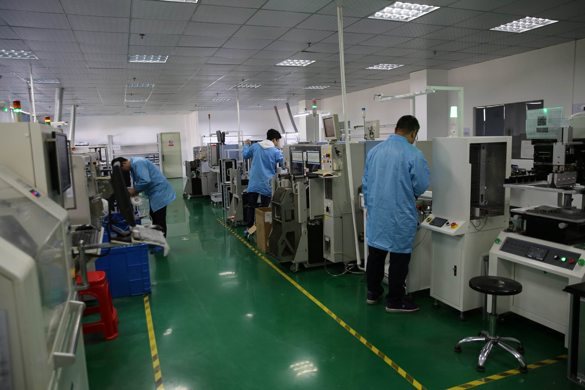
At Bester, we are proud to offer top-notch PCB fabrication services to our valued customers. With years of experience and expertise in the field, we are committed to delivering high-quality printed circuit boards that meet the unique requirements and specifications of our clients. Our state-of-the-art manufacturing facility is equipped with advanced technology and cutting-edge machinery that enables us to produce PCBs with precision and accuracy. We have a team of skilled engineers and technicians who work diligently to ensure that every step of the fabrication process is carefully executed, from the initial design to the final production. With a strong focus on quality control, we implement rigorous testing procedures to guarantee the reliability and functionality of each PCB we manufacture. Whether it’s a small-scale project or a large-scale production run, we have the capacity and capability to handle any order size.
PCB Fabrication Process
There is no such thing as a standard printed circuit board. Each PCB has a unique function for a particular product. Therefore, producing a PCB is a complex process of many steps. This overview covers the most important steps when producing a multilayer PCB. When you order PCBs from Bester Tech, you are buying quality that pays for itself over time. This is guaranteed through a product specification and quality control that is far more stringent than other suppliers, and ensures that the product delivers what it promises. In the production flow below you can see where the process is unique or goes beyond the IPC standard.
Pre Production
We use the data (Gerber file) you provide to create the production information for your customized boards. Our experts match your specifications with the capacities for compliance purposes.
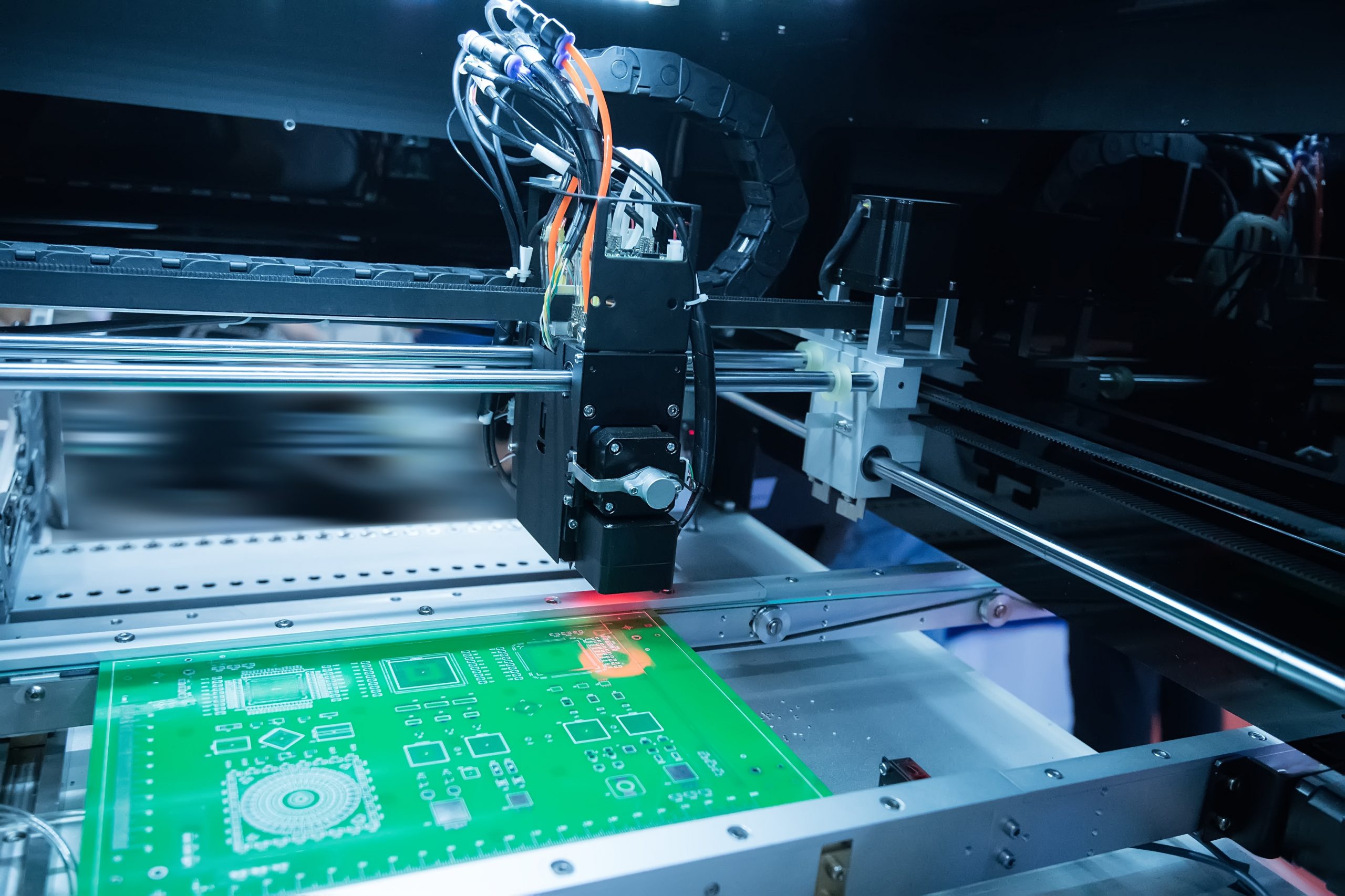
Inner Layer Imaging
When making circuit board, the imaging process is what defines the circuit traces. Traditional imaging process needs a UV-light and photo-tool to transfer images, while LDI only uses a computer-controlled, highly focused, laser beam to directly define the circuit pattern onto the board.
Inner Layer Etching
Leverage the etching process to eliminate any undesirable copper residues from the panel. After removal, we remove the dry film to remain with copper circuitry as well, which is in line with the PCB design.
Inner Layer AOI
Inspection of the circuitry against digital images to verify that the circuitry matches the design and that it is free from defects. Achieved through scanning of the board and then trained inspectors will verify any anomalies that the scanning process has highlighted.
Lamination
Apply an oxide layer to the inner board layers and then stack them together using prepreg to create insulation between them. Copper foil is added to the upper and lower stack parts.
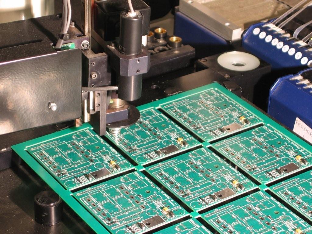
PCB Drilling
Bore the holes that will later act as electrical contacts in the multilayer board. Drilling is a mechanical process that PCB manufacturers optimize to obtain registration to the internal layer links.
Electroless Copper Deposition
Apply thin copper layer deposits on the holes that drilled earlier on the walls. PTH offers copper deposits, which conceal the hole walls and the whole panel.
Outer Layer Imaging
Outer layer imaging resembles the internal layering process. However, in outer layer drilling, get rid of the dry film and maintain the circuitry. Then plate the extra copper later in a clean environment.
Graphic Plating
The second electrolytic plating process, where we carry out extra plating in dry film parts (circuitry). After depositing the copper, we should apply tin to prevent the plated copper from oxidation.
Outer Layer Etching
Take out the dry blue film and scrape all the unwanted copper residues. The tin deposits resist the etching process to protect the copper deposit, then chemically eliminated the tin residues to leave behind the circuitry.
焊接掩模
With the help of artwork and Ultraviolet light, expose some PCB parts and remove all the exposed parts. Then completely cure the remaining solder mask to create a quality finish.
表面处理
Surface finish can maintain the exposed copper circuitry meanwhile provide a solderable surface when soldering components to the PCB. Metallic and organic are the two main kinds of surface finishes.
电气测试
Test all boards before shipping to ensure all of the printed circuit boards are free of defects and meet the standards you expect. Test including flying probe, fixtureless testers. And we also have universal grid testing capability. These machines use fixtures built specifically for your PCB.
Profiling
Route the PCB production panels into particular sizes and shapes according to the production file. PCB V-Scoring is a process of cutting a ‘V’ shaped groove at the top and bottom of a printed circuit board, leaving a thin layer between the Vees. Once we have done this, it can easily separate the PCB Board at the V by applying minimal pressure.
Final Visual Inspection
A team of sharp-eyed individuals scrutinizes each product. The process involves visually examining the board in line with the set standards.
Rapid PCB Prototyping and Small-volume Production
Our state-of-the-art assembly equipment enables us to meet all your PCBA needs under one roof in an inexpensive way, our Printed Circuits Boards Assembly Capability includes but not limited to what are listed below, as we are updating our equipment constantly to keep us on the cutting edge.
- 电路板规格
- Maximum Panel size: 19.7″ x 31.5″, Maximum Number of Layers: 1-40, Copper Thickness: 0.5 oz to 5.0 oz, Minimum Line Width: 3 mil, Minimum Line spacing: 3 mil, Smallest Hole: 0.006″, Blind, Buried and plugged Vias, Controlled impedance
- 材料
- Thickness: 0.008″ to 0.240″, FR-4, High TG FR-4, PTFE, Aluminum Base, Rogers, Specialized material per your request
- 焊接掩模
- LPI – Green, Yellow, Black, Red, Blue, White, etc. (Inquire for more options), Peelable Mask
- 最终完成
- SMOBC (HASL), Carbon, Selective Gold Plating, Hard and Soft Gold, Immersion Gold, Immersion Silver, Immersion Tin, OSP
- 图例
- 白色、黄色、黑色(如需更多选择,请咨询)
- 检查方法
- 100% Visual inspection, Electrical testing – Flying probe or Nails Bed, Sample lot inspection, Cross sectioning
- 送货
- Rush: 24 Hours, Standard Prototype: 5 days, Standard Production: 10 days
为什么选择 Bester

强大的装配能力
我们拥有最先进的设施和技术精湛的团队,有能力处理最复杂的 PCB 组装项目,确保高效、准确地制造您的产品。

质量保证
我们严格的质量控制流程和广泛的测试程序确保我们生产的每个 PCB 组件都符合可靠性和性能方面的最高行业标准,让您对我们的服务放心和充满信心。

一站式服务
从 PCB 制作和设计到元件采购和 IC 编程,Bester 在同一屋檐下为您提供全面的服务,简化生产流程,节省您的时间和精力。

快速周转
我们对快速周转时间的承诺意味着您的印刷电路板组装项目将如期完成,使您能够在截止日期前完成生产,并迅速将产品推向市场。
客户和认证

Bester 的电子制造能力
制造能力
- 100% ESD 元件控制装置
- 8 条 SMT 线
- 4 个 DIP 线路
- 40 自动机器人焊接
- 数控加工
- 自动保形涂料
- 注塑成型
- 三维打印
认证
- ISO 9001
- UL
- SGS
- IPC
- RoHS
- CE
- 联邦电信交通委员会
- SRDI(中国 "专精特新 "企业)
- HNTE(中国高新技术企业)
我们服务的行业

汽车
我们深知 PCBA 在汽车行业中的关键作用。我们提供全面的 PCBA 服务,满足汽车制造商的特定需求,帮助他们提供可靠、高性能的电子系统。
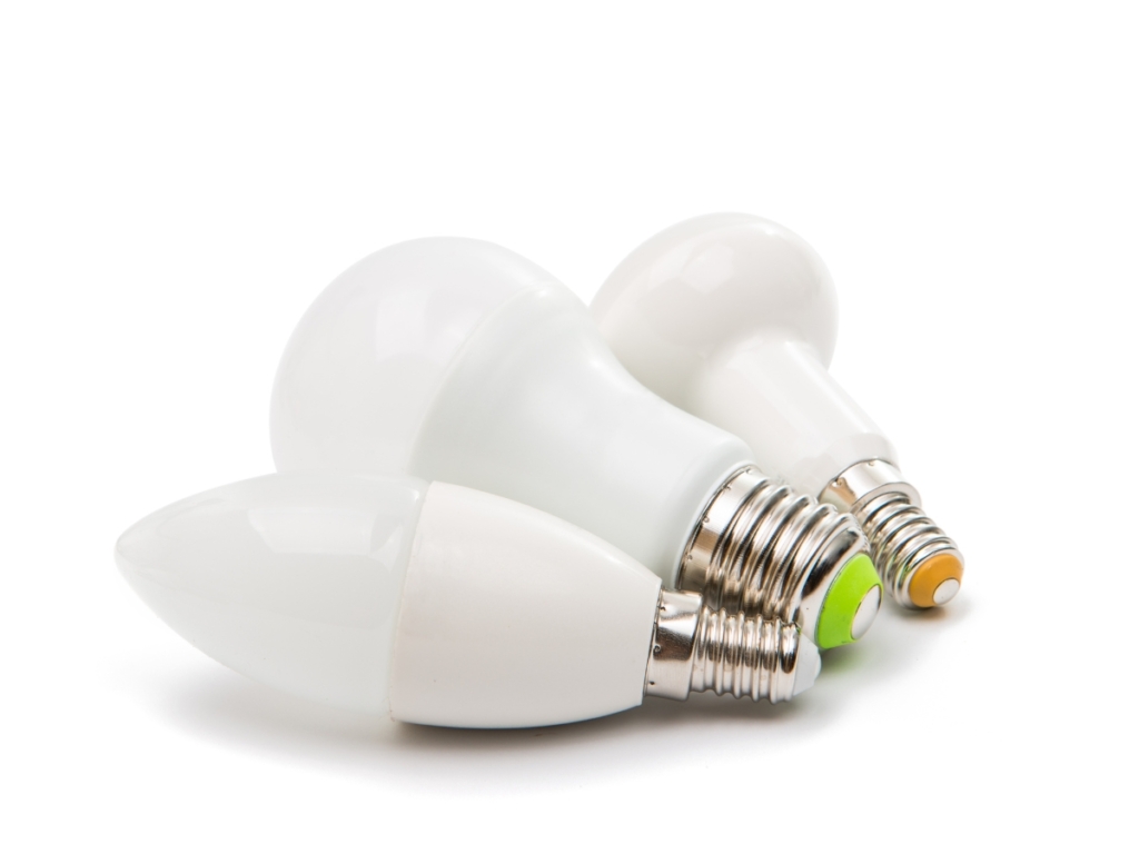
发光二极管
在 LED 市场,Bester 提供一流的 PCBA 解决方案,这对生产高质量的 LED 照明产品至关重要。我们与 LED 制造商密切合作,确保他们的 PCBA 符合能效、耐用性和性能方面的严格要求。
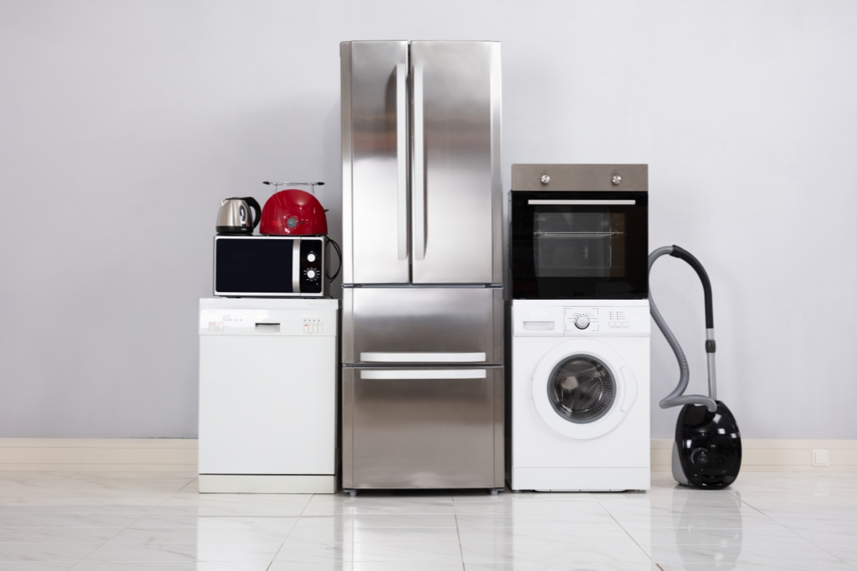
消费电子产品
Bester 通过提供广泛的 PCBA 服务来满足消费电子市场的需求,从而生产出创新的、用户友好的电子设备。我们与消费电子产品制造商合作,确保他们的 PCBA 符合最高的质量和功能标准。

工业
在工业领域,Bester 的 PCBA 服务在开发可靠、高效的电子系统方面发挥着至关重要的作用。我们与工业设备制造商密切合作,以满足他们的特定要求,确保我们的 PCBA 能够承受恶劣的环境条件,并提供最佳性能。
pcba 应用
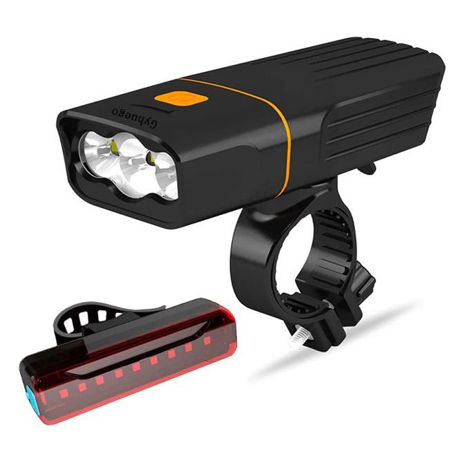
自行车灯 PCBA
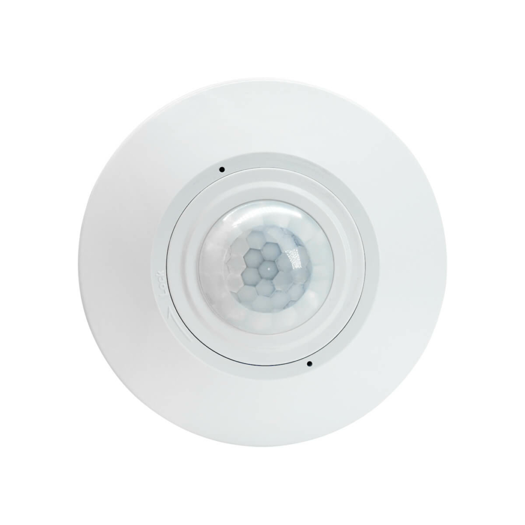
PIR 移动传感器 PCBA
LED PCBA
PCB Manufacturing FAQ
如何获得标准印刷电路板的报价
只需点击或拨打一个电话,即可获得免费的 PCB 报价。请给我们发送电子邮件或致电,以获得最快速的报价。
使用 Bester 制作 PCB 的优势
Bester 是一个提供全方位服务的交钥匙 PCB 解决方案,可以处理从原型到制造再到组装的所有工作。十多年来,我们一直在制造高质量的标准 PCB,并完全符合 ISO9001:2015 质量标准。我们的所有标准印刷电路板均符合 IPC2 标准,并进行严格的内部质量保证测试,以确保运抵您工厂的电路板值得信赖。
我们提供符合您预算的 PCB 解决方案。您可以订购几块原型板来测试您的设计,然后批量订购标准印刷电路板,以节省更多费用。我们将为您提供免费的即时报价,让您了解自己的期望值,从而制定相应的计划。我们还提供来自 PCB 专家的全面技术支持。如有任何问题,请致电我们、在线聊天或发送电子邮件给我们,无论哪种方式对您来说最方便。我们会尽快处理您的疑虑或问题。我们已获得 99% 以上的客户满意度,只要您开始订购印刷电路板,我们就会立即为您提供服务。

准备好开始您的 PCB 组装项目了吗?