What is Traces and Spaces
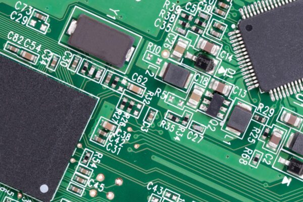
Traces and Spaces, in the context of the PCB industry, refer to the width and spacing of the conducting copper lines on a printed circuit board (PCB). Traces are the thin lines of conducting copper that carry electrical signals between components on the PCB, while spaces refer to the gaps or distances between these traces.
The width of a trace is an important factor as it determines its current carrying capacity and other characteristics. The cross-sectional area of a trace, which is directly proportional to its width and copper thickness, determines how much current it can safely carry. Power traces typically require wider widths to accommodate higher current flow, while signal traces may have different width requirements based on specific design considerations.
The spacing between traces is crucial for minimizing crosstalk, coupling, reflections, and signal distortion. Adequate spacing helps prevent interference between adjacent traces and ensures the integrity of the signals being transmitted. Different types of routing, such as digital and analog, may require specific trace widths and spacings based on the particular requirements of the circuitry.
It is worth noting that trace width and spacing considerations also take into account manufacturing constraints. Fabricators have their own minimum trace width and spacing requirements to prevent shorts during fabrication. Additionally, the copper weight used in a specific layer of the PCB can influence the minimum trace width achievable during fabrication.
Frequently Asked Questions
How Much Current Can PCB Traces Handle
PCB design textbooks and IPC standards provide comprehensive information on the dc current-carrying capability of PCB traces, typically up to approximately 30A. However, there is limited reference material available beyond this threshold, both in terms of current and frequency.
What Is the Difference Between Trace and via in PCB
Vias are essentially conductive holes on a PCB that establish electrical connections between different layers, such as connecting the top and bottom layers or layers in between. In contrast, traces are designed to conduct electricity between PCB components or pads.
How Close Can Traces Be to Edge of PCB
Keep traces at a minimum distance of 0.025″ from the deepest edge of the mouse bite. It is crucial to consider and incorporate PCB board edge clearance requirements into your design process. These regulations apply to all aspects of PCB manufacturing, such as components, connectors, drill holes, and traces.
What Happens if Trace Width Is Too Small
Traces that are used to route power and ground require a wider width in order to effectively conduct larger amounts of current. If the traces are too narrow, there is a risk of overheating and potential burn-through.
Are Wider Traces Better
Ground and power traces typically carry higher currents, which means they need to be wider. Thin traces can have higher resistance and may even burn through. To ensure proper heat dissipation, it is important for ground and power traces on the inner layers to be wider.
