What is Mask
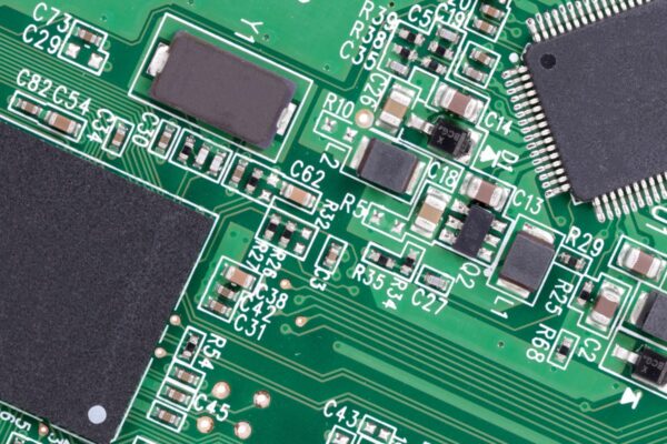
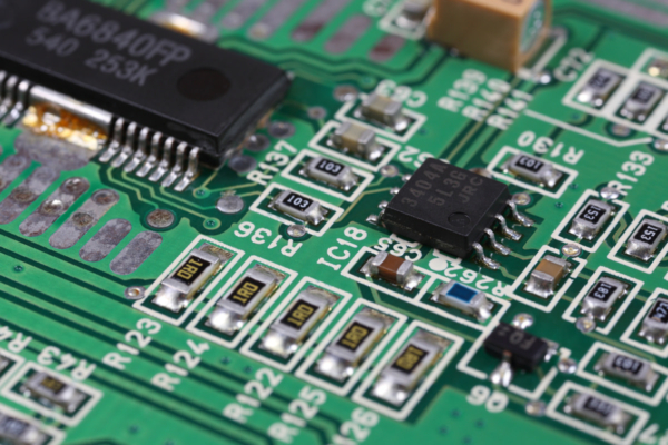
Mask refers to the soldermask, which is a protective layer applied to a PCB. The soldermask is a liquid photo imageable lacquer that is applied to the top and bottom sides of the PCB. It protects the copper traces on the PCB, excluding the solder pads, from various factors that can affect their performance and reliability.
The soldermask serves as a barrier against oxidation, preventing the copper traces from being damaged. It also helps prevent shorts during the soldering process, such as solder bridges, by providing insulation between adjacent traces. It protects the PCB from external conductive influences and high voltage spikes that could disrupt its operation.
The application of the soldermask involves printing or spraying it onto the production panel and then exposing it to UV light with the correct solder mask pattern. After exposure, the soldermask is developed and dried. While the soldermask is typically green, it can also be applied in other colors like black, blue, white, red, or clear.
The thickness of the soldermask varies depending on the location on the PCB. For example, on conductor side edges and conductor top, the minimum thickness is specified to be greater than 7 microns (t1 and t2). The maximum soldermask thickness can be up to 40µm for a 35µm finished copper thickness, and for higher final copper thicknesses, it can be up to 80µm.
The soldermask is allowed to encroach on lands as long as the minimum annular ring requirements are maintained. It is not permitted in plated through holes (PTH) that are not intended for solder fill. Isolated pads should not be exposed, and there should be no soldermask encroachment on edge board connector fingers or test points. The extent of encroachment on SMT-pads depends on their pitch, with a maximum encroachment of 50 microns (2 mil) for pads with a pitch of 1.25 mm or more, and 25 microns (1 mil) for pads with a pitch less than 1.25 mm.
