What is Layer
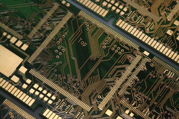
A layer refers to a copper layer within a PCB. PCBs are constructed with multiple copper layers arranged in a predetermined sequence. These copper layers, also known as “signal layers,” carry electrical signals, facilitate wiring, and enable component placement within the PCB.
Apart from the signal layers, there are other layers in a PCB that serve different functions. These layers are typically named based on their position and functionality within the PCB. For instance, there are layers such as the top solder mask layer, top paste layer, top legend layer, bottom peel-off layer, and more.
The number of copper layers present in a PCB is used to classify and identify the board. PCBs with a single copper layer are referred to as “1-layer PCBs” or “single-sided PCBs,” while those with two copper layers are known as “2-layer PCBs” or “double-sided PCBs.” PCBs with more than two copper layers are designated by the specific number of copper layers they possess, such as “4-layer PCBs” or “6-layer PCBs.”
