What is Laser Direct Imaging
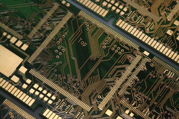
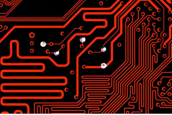
Laser direct imaging (LDI) is a technology used to define copper circuit patterns directly on PCBs. Unlike traditional methods that rely on phototools and UV light, LDI utilizes a computer-controlled, highly concentrated laser beam to create the circuit patterns on the PCB’s copper layers covered with laser photoresist.
The process of LDI involves exposing the circuit patterns from a Gerber file onto a photoresist film using a UV laser beam. This exposure is done incrementally across the laminate in a raster manner, similar to the lines on a computer screen. The resulting image is highly accurate and precise, allowing for the creation of fine lines and intricate designs.
LDI offers several advantages over traditional photolithography methods. It eliminates the need for phototools, reducing production time and costs. It also provides improved image quality, accurate positioning, and reduced environmental impact. Additionally, LDI enables the production of more complex and intricate designs, as it can create finer lines and smaller features.
