What is Imaging
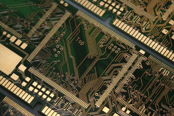
Imaging is the process of defining the copper circuit patterns on a printed circuit board and determining the layout and functionality of the circuits.
Traditionally, the imaging process in PCB manufacturing involved using UV light and a phototool to transfer circuit images onto the PCB. However, with advancements in technology, a more efficient and precise method known as laser direct imaging (LDI) has emerged.
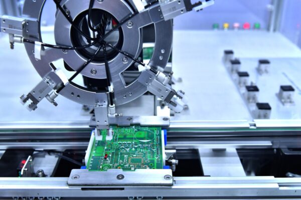
LDI technology utilizes a computer-controlled, highly concentrated laser beam to directly expose the circuit patterns onto the PCB’s copper layers covered with laser photoresist. This eliminates the need for a phototool and allows for more accurate and intricate circuit designs.
The LDI process begins with converting the circuit design into a Gerber file containing the necessary information for the laser to create the circuit patterns. The UV photoresist, specifically designed for laser printing, is selectively exposed to the UV laser beam in increments across the laminate in a raster manner. This exposure creates the circuit patterns on the photoresist film, which can be compared to the image displayed on a computer screen.
Compared to traditional photolithography, LDI offers several advantages. It provides improved precision, efficiency, and flexibility, making it a preferred choice for PCB manufacturers, especially for high-density interconnect (HDI) PCBs with fine lines and complex interconnections. LDI technology eliminates the limitations and challenges associated with traditional imaging methods, allowing for more accurate and intricate circuit designs.
