What is High Density Interconnect (HDI)
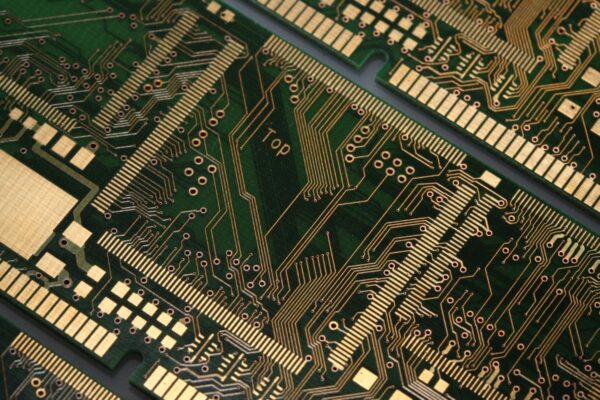
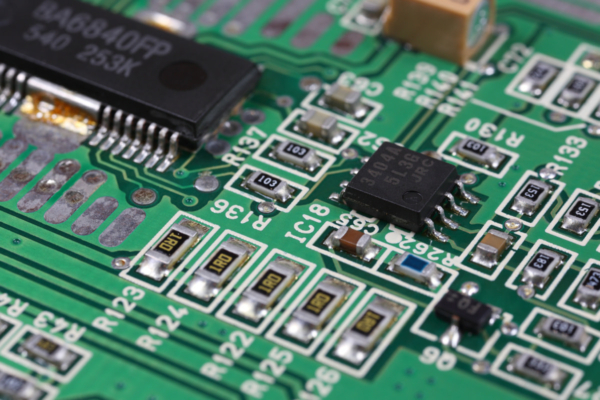
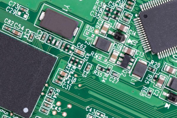
High Density Interconnect (HDI) describes a type of printed circuit board that achieves a higher wiring density per unit area compared to traditional PCBs. HDI PCBs are designed to meet the growing demand for smaller, faster electronic products.
HDI PCBs incorporate various features to achieve their high density. These features include microvias, blind and buried vias, built-up laminations, and considerations for high signal performance. Microvias are small holes drilled into the PCB that allow for the routing of traces between different layers, while blind and buried vias connect the outer layers of the board to internal layers. These features enable the placement of a large number of components and interconnections in a smaller space.
HDI PCBs allow for the consolidation of multiple traditional PCBs into a single HDI PCB, resulting in lighter weight, more compact, and lower layer count boards. The smaller vias, pads, copper traces, and spaces in HDI PCBs enable denser wiring, which leads to improved performance and reduced power consumption. Additionally, HDI PCBs offer better signal integrity, lower RFI/EMI, and distributed capacitance.
HDI PCBs find applications in various industries and electronic devices that require high performance in a limited space, including mobile phones, laptops, digital cameras, network communications, automotive and aerospace industries, medical devices, industrial automation, and the Internet of Things (IoT).
Frequently Asked Questions
What Are the Different Types of HDI PCBs
IPC-2226 defines HDI as a printed circuit board with a higher wiring density per unit area compared to conventional PCBs. IPC-2226 also categorizes HDI features into three types: type I, type II, and type III. For more information on these different types, please refer to our FAQ section.
What Is the Difference Between HDI and Non HDI PCB
HDI PCBs, in comparison to traditional PCBs, offer the advantage of accommodating higher component density on smaller and lighter boards. Additionally, HDI PCBs typically have fewer layers. This is achieved through the utilization of laser drilling, micro vias, and lower aspect ratios on the vias, distinguishing them from standard circuit boards.
