What is HDI PCB
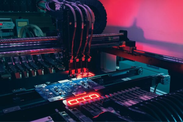
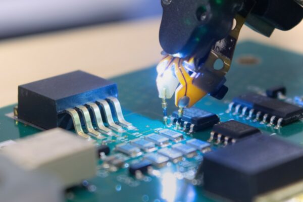
HDI PCB, or High-Density Interconnect Printed Circuit Board, is designed to maximize space utilization while maintaining circuit functionality. It achieves this through a higher number of interconnections, allowing for a more compact design and miniaturization of the board. HDI PCBs typically have a high pin density, achieved through advanced design techniques and technologies such as microvias, buried vias, and blind vias.
Microvias are small holes drilled into the PCB that enable signal routing between different layers, allowing for denser circuitry and more interconnections in a smaller area. Buried vias are located between inner layers and provide additional routing options without occupying space on the outer layers. Blind vias connect the outer layers to inner layers, enabling efficient routing between specific layers without affecting the entire board.
HDI PCBs offer advantages such as improved signal integrity, efficient routing options, and reduced drill to copper ratio. They are commonly used in applications where space is limited, such as portable electronic devices and high-performance systems. The healthcare, consumer electronics, aerospace, and wearables industries have all adopted HDI PCB technology.
