What is Fully-Additive Process
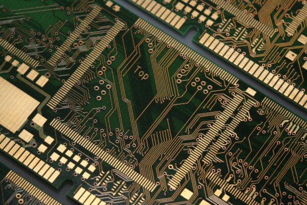
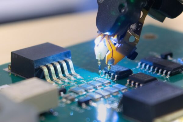
A fully-additive process is a manufacturing technique used to build PCBs. Unlike traditional methods that involve subtractive processes such as etching, the fully-additive process is characterized by the addition of material without any subtraction. This is achieved through a combination of 3D printing and chemical deposition techniques.
In the fully-additive process, all layers of the PCB, including the substrate and conductors, are added on rather than being etched away. This approach offers several advantages, including a highly automated production flow and the ability to create precise patterns on surfaces. Additionally, the fully-additive process operates at a lower temperature compared to traditional methods, typically around 150°C.
The fully-additive process has gained attention in the PCB industry due to its potential for developing smaller form factor electronics and its suitability for applications such as RF antennas and 5G technology. By enabling the creation of intricate patterns and structures, the fully-additive process allows for the production of high-performance PCBs with improved efficiency and reduced power consumption.
