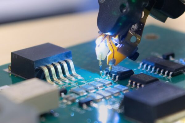
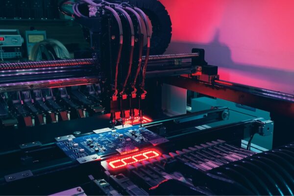
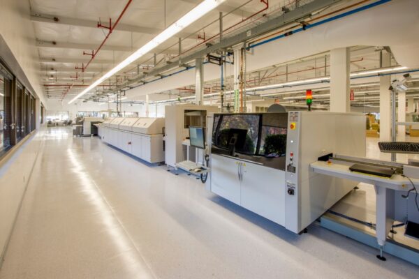
The demand for compact, lightweight, and adaptable circuit boards has never been higher. Enter the flexible printed circuit board, a technology that has revolutionized the way we design and manufacture electronic devices. With their ability to bend, fold, and conform to various shapes, flexible PCBs have opened up a world of possibilities for engineers and designers alike. In this comprehensive guide, we will delve into the intricacies of flexible PCBs, exploring their unique characteristics, types, advantages, and diverse applications across industries.
What is a Flexible PCB
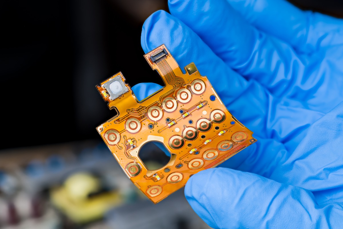
A flexible PCB, also known as a flex circuit or flexible printed circuit, is a specialized type of printed circuit board that consists of a thin, flexible substrate with conductive traces etched onto its surface. Unlike traditional rigid PCBs, which are made from a solid, inflexible material like fiberglass, flexible PCBs utilize a pliable polymer substrate, typically polyimide or polyester. This flexibility allows the circuit board to bend, fold, and conform to various shapes, making it ideal for applications where space is limited or where the device needs to adapt to irregular surfaces.
The basic structure of a flexible PCB consists of three main components: the dielectric substrate film, conductive layers, and protective coverlay. The dielectric substrate film, usually made from polyimide (PI) or polyethylene terephthalate (PET), provides electrical insulation and mechanical support for the conductive layers. The conductive layers, typically made from copper, are etched onto the substrate to create the desired circuit pattern. The copper can be either electrodeposited (ED) or rolled annealed (RA), depending on the application requirements. A thin layer of insulating material, often polyimide or a flexible solder mask, is applied over the conductive layers to protect them from damage and environmental factors.
In addition to these basic components, flexible PCBs may also incorporate adhesive materials for bonding layers together, as well as stiffeners in certain areas to provide additional support for components or connectors. The key characteristics that set flexible PCBs apart from their rigid counterparts are their flexibility, thinness, and lightweight nature. These properties enable flex circuits to be used in applications where traditional rigid PCBs would be impractical or impossible. Flexible PCBs can withstand repeated bending and folding without compromising their electrical performance, making them highly durable and reliable in dynamic environments.
Note that flexible PCBs can be combined with rigid PCBs to create hybrid designs known as rigid-flex PCBs. These boards incorporate both flexible and rigid sections, allowing for even greater design flexibility and functionality. Rigid-flex PCBs are particularly useful in applications where the circuit board needs to transition between fixed and movable components, such as in folding smartphones or medical devices.
Types of Flexible PCBs
Flexible PCBs come in various configurations, each designed to meet specific application requirements. They can be classified based on their layer configuration and design configuration.
Layer Configuration
Flexible PCBs can be single-sided, double-sided, or multilayer. Single-sided flexible circuits are the simplest and most cost-effective type, consisting of a single conductive layer on one side of the flexible substrate. They are ideal for applications that require a low component density and minimal complexity, such as in simple sensors or interconnects. Double-sided flexible circuits have conductive layers on both sides of the substrate, connected by plated through-holes (PTHs). They offer increased circuit density and power-handling capabilities compared to single-sided designs and are commonly used in applications such as digital cameras, mobile devices, and computer peripherals. Multilayer flexible circuits consist of three or more conductive layers, separated by insulating layers and interconnected by PTHs. They are designed for applications that demand high circuit density, such as in aerospace, military, and advanced medical devices. While they offer superior performance, multilayer flex circuits are also more expensive and challenging to manufacture than their single or double-sided counterparts.
Design Configuration
Flexible PCBs can also be classified based on their design configuration, such as rigid-flex PCBs and High Density Interconnect (HDI) flexible PCBs. Rigid-flex PCBs combine the benefits of both rigid and flexible PCBs, consisting of one or more rigid PCB sections connected by flexible PCB sections. This configuration allows for three-dimensional packaging and improved reliability, as the flexible sections eliminate the need for connectors or wires between rigid boards. Rigid-flex PCBs are widely used in consumer electronics, automotive systems, and medical devices. HDI flex circuits are designed to accommodate extremely dense circuitry with fine features and micro vias. These advanced flex circuits offer superior electrical performance and miniaturization capabilities compared to standard flexible PCBs. HDI flex circuits are essential in applications that require high-speed signal transmission, such as in 5G communication devices or advanced wearable electronics.
Others
In addition to these main categories, there are also specialized types of flexible PCBs, such as sculptured flex circuits and component-integrated flexible circuits. Sculptured flex circuits feature varying thicknesses of the conductive layers, allowing for controlled impedance and enhanced flexibility in specific areas. Component-integrated flexible circuits, on the other hand, have electronic components directly embedded into the flexible substrate, resulting in an ultra-thin and compact package.
Advantages of Flexible PCBs
Flexible PCBs offer numerous advantages over traditional rigid PCBs, making them an attractive choice for a wide range of applications.
Flexibility and Conformability
The most obvious advantage of flexible PCBs is their ability to bend, fold, and conform to tight spaces and irregular shapes. This flexibility enables designers to create more compact and ergonomic devices, as the circuit board can adapt to the available space rather than dictating the device’s form factor.
Weight Reduction
Flexible PCBs are significantly lighter than their rigid counterparts, often weighing up to 75% less. This weight reduction is crucial in applications where every gram counts, such as in aerospace, drones, and wearable devices.
Space-Saving in 3D Applications
The conformability of flexible PCBs allows for three-dimensional packaging, enabling designers to make the most of the available space within a device. This is particularly valuable in applications where space is at a premium, such as in smartphones, smartwatches, and medical implants.
Improved Reliability
Flexible PCBs often require fewer interconnections than rigid PCBs, as the flexible sections can directly connect components without the need for connectors or wires. This reduction in interconnections leads to improved reliability, as there are fewer potential points of failure.
Better Thermal Management
The thin, lightweight nature of flexible PCBs allows for better heat dissipation compared to rigid PCBs. This improved thermal management can help extend the lifespan of electronic components and prevent overheating in compact devices.
Resistance to Vibration and Shock
The flexibility of flex circuits enables them to withstand vibration and shock better than rigid PCBs. This is particularly important in applications that are subject to harsh environments, such as in automotive, aerospace, and industrial settings.
High-Density Packaging Capabilities
Flexible PCBs can accommodate high-density component placement, thanks to their ability to conform to tight spaces and the availability of HDI flex circuit technology. This enables designers to create more compact and feature-rich devices without compromising on performance.
Reduced Assembly Time and Costs
By eliminating the need for connectors and wires between boards, flexible PCBs can simplify the assembly process and reduce overall manufacturing costs. This is especially true for rigid-flex PCBs, which integrate both rigid and flexible sections into a single, unified board.
Improved Product Design Freedom
The flexibility and conformability of flex circuits give designers greater freedom to create innovative and aesthetically pleasing products. Flexible PCBs can enable unique form factors and designs that would be impossible with rigid PCBs alone.
Enhanced Durability in Dynamic Flexing Applications
In applications that require repeated bending or flexing, such as in hinges or folding mechanisms, flexible PCBs offer superior durability compared to rigid PCBs or traditional wiring. The ability to withstand dynamic flexing without compromising electrical performance makes flex circuits ideal for these demanding applications.
Ability to Replace Bulky Wire Harnesses
Flexible PCBs can often replace complex and bulky wire harnesses, simplifying the overall system design and reducing weight and space requirements. This is particularly valuable in automotive and aerospace applications, where wiring can account for a significant portion of the overall system weight.
Disadvantages of Flexible PCBs
Despite their numerous advantages, flexible PCBs also have some drawbacks that designers must consider when deciding whether to use them in a particular application.
Higher Initial Costs
Compared to rigid PCBs, flexible PCBs often have higher initial design and manufacturing costs. This is due to the specialized materials, processes, and equipment required to produce flex circuits. The higher costs can be a barrier for some applications, particularly those with tight budget constraints or low production volumes.
More Complex Design Process
Designing flexible PCBs requires a deeper understanding of the materials, mechanical properties, and manufacturing processes involved. Designers must consider factors such as bend radius, material selection, and layer stack-up to ensure the flex circuit will perform reliably in the intended application. This complexity can lead to longer design cycles and the need for specialized expertise.
Potential for Damage During Handling or Assembly
The thin and flexible nature of flex circuits makes them more susceptible to damage during handling and assembly compared to rigid PCBs. Proper care must be taken to avoid creasing, tearing, or stretching the flex circuit, which can lead to electrical failures or reduced reliability.
Limited Availability of Manufacturers
While the demand for flexible PCBs has grown in recent years, not all PCB manufacturers have the capabilities or expertise to produce high-quality flex circuits. This limited availability can make it more challenging to find a suitable supplier, particularly for complex or high-volume projects.
Challenges in Repairing or Modifying
Once a flexible PCB has been manufactured, it can be more difficult to repair or modify compared to a rigid PCB. The flexible substrate and protective layers must be carefully removed and reapplied to access the conductive layers, which can be a delicate and time-consuming process.
Potential Issues With Signal Integrity
In high-frequency applications, the flexible nature of the substrate can lead to signal integrity issues if not properly designed and controlled. Factors such as impedance matching, crosstalk, and electromagnetic interference (EMI) must be carefully considered to ensure reliable performance.
Limited Component Placement Options
While flexible PCBs can accommodate high-density component placement, the flexible nature of the substrate can limit the size and type of components that can be used. Heavy or large components may require additional support or stiffening to prevent damage to the flex circuit during bending or flexing.
Applications of Flexible PCBs
Flexible PCBs have found widespread use across a diverse range of industries, thanks to their unique properties and advantages.
Consumer Electronics
The consumer electronics industry has been one of the primary drivers of flexible PCB adoption. Flex circuits are extensively used in smartphones, tablets, and wearable devices, such as smartwatches and fitness trackers. In these applications, flexible PCBs enable compact, lightweight, and ergonomic designs that can conform to the device’s housing and withstand the stresses of daily use. For example, in a smartwatch, a flexible PCB can be bent to fit the contours of the watch case, allowing for a more comfortable and stylish design.
Automotive Industry
Flexible PCBs play a crucial role in modern automotive electronics, where they are used in applications such as dashboard displays, airbag systems, and engine control modules. The ability of flex circuits to withstand vibration, shock, and extreme temperatures makes them ideal for the harsh environment of a vehicle. In an airbag system, for instance, a flexible PCB can be folded and placed in the steering wheel, allowing for reliable deployment in the event of a collision.
Medical Devices
The medical device industry has embraced flexible PCBs for their ability to conform to the human body and enable miniaturized, implantable devices. Flex circuits are used in pacemakers, hearing aids, and ultrasound probes, among other medical applications. In a pacemaker, a flexible PCB can be folded to fit within the compact titanium housing, while still providing reliable electrical connections to the battery and sensors. The biocompatibility and durability of flex circuits make them suitable for long-term implantation and exposure to bodily fluids.
Aerospace and Defense
Flexible PCBs are essential in aerospace and defense applications, where weight reduction, space savings, and reliability are paramount. Flex circuits are used in satellites, aircraft control systems, and military communication devices, where they can replace heavy and bulky wiring harnesses. In a satellite, for example, flexible PCBs can be used to interconnect various subsystems, such as power management, data processing, and communication modules, while minimizing weight and volume.
Industrial Applications
In industrial settings, flexible PCBs are used in a wide range of applications, including robotics, flexible solar panels, and 3D printers. The ability of flex circuits to withstand repeated flexing and harsh environmental conditions makes them suitable for use in industrial automation and control systems. In a robotic arm, flexible PCBs can be used to route signals and power between the various joints and actuators, enabling smooth and precise motion control.
Materials Used in Flexible PCBs
The choice of materials used in flexible PCBs is critical to their performance, reliability, and durability. The main components of a flexible PCB include the base substrate, conductive layers, coverlay, adhesives, and surface finishes.
Base Materials (Substrates)
The base material, or substrate, is the foundation of a flexible PCB, providing electrical insulation and mechanical support for the conductive layers. The most common base materials used in flex circuits are:
- Polyimide (PI): PI is the most widely used substrate material for flexible PCBs, thanks to its excellent thermal stability, chemical resistance, and mechanical properties. PI can withstand high temperatures (up to 400°C) and has a relatively low coefficient of thermal expansion (CTE), making it suitable for applications with demanding environmental conditions.
- Polyethylene Terephthalate (PET): PET is a lower-cost alternative to PI, offering good electrical properties and flexibility. However, PET has a lower temperature resistance compared to PI, limiting its use in high-temperature applications.
- Polyethylene Naphthalate (PEN): PEN is a high-performance substrate material that offers better thermal and mechanical properties than PET, but at a higher cost. PEN is often used in applications that require a balance between performance and cost.
Conductive Materials
The conductive layers in a flexible PCB are responsible for carrying electrical signals and power between components. The most common conductive materials used in flex circuits are:
- Copper: Copper is the most widely used conductor in flexible PCBs, thanks to its excellent electrical conductivity, thermal conductivity, and mechanical properties. There are two main types of copper used in flex circuits:
- Electrodeposited (ED) copper: ED copper is deposited onto the substrate using an electroplating process, resulting in a thin and uniform layer. ED copper is often used in high-density designs and HDI applications.
- Rolled Annealed (RA) copper: RA copper is produced by mechanically rolling and annealing copper foil, resulting in a thicker and more ductile layer. RA copper is preferred in applications that require repeated flexing or bending, as it offers better fatigue resistance compared to ED copper.
- Aluminum: Aluminum is sometimes used as an alternative to copper in flexible PCBs, particularly in applications that require lightweight and low-cost solutions. However, aluminum has lower electrical and thermal conductivity compared to copper, limiting its use in high-performance applications.
- Silver ink: Silver-based conductive inks are used in some flexible PCB applications, particularly in printed electronics and wearable devices. Silver inks can be screen-printed or inkjet-printed onto flexible substrates, enabling the creation of thin and stretchable circuits.
- Other specialized conductors: In some niche applications, other conductive materials such as Constantan (copper-nickel alloy) or Inconel (nickel-chromium-based superalloy) may be used for their specific properties, such as high resistance or corrosion resistance.
Coverlay and Protective Materials
Coverlay and protective materials are used to insulate and protect the conductive layers in a flexible PCB. The most common materials used for this purpose are:
- Polyimide film: PI film is often used as a coverlay material, providing excellent insulation, mechanical protection, and flexibility. PI coverlay is typically bonded to the conductive layers using adhesives.
- Flexible solder mask: Flexible solder mask is a photoimageable polymer coating that is applied over the conductive layers to protect them from oxidation and prevent short circuits during soldering. Flexible solder mask also helps to define the solderable areas on the flex circuit.
- Covercoat materials: Covercoat materials are thin, protective coatings that are applied over the conductive layers to provide insulation and environmental protection. Common covercoat materials include acrylic, polyurethane, and silicone-based coatings.
Adhesives
Adhesives are used in flexible PCBs to bond the various layers together, ensuring mechanical stability and reliability. The two main types of adhesives used in flex circuits are:
- Acrylic: Acrylic adhesives offer good bonding strength, flexibility, and chemical resistance. They are often used to bond the coverlay or protective films to the conductive layers.
- Epoxy: Epoxy adhesives provide excellent mechanical strength and thermal stability, making them suitable for applications with demanding environmental conditions. Epoxy adhesives are often used to bond the substrate layers together in multilayer flex circuits.
Surface Finishes
Surface finishes are applied to the exposed copper pads on a flexible PCB to protect them from oxidation and enhance solderability. The choice of surface finish depends on the specific application requirements, such as environmental conditions, shelf life, and assembly process. Common surface finishes used in flex circuits include:
- ENIG (Electroless Nickel Immersion Gold): ENIG is a two-layer surface finish that consists of a thin layer of gold over a nickel barrier layer. ENIG offers excellent solderability, corrosion resistance, and shelf life, making it a popular choice for high-reliability applications.
- HASL (Hot Air Solder Leveling): HASL is a tin-lead or lead-free solder coating that is applied to the copper pads and then leveled using hot air. HASL provides good solderability and is a cost-effective option for many applications.
- Immersion Tin: Immersion tin is a single-layer surface finish that is applied directly onto the copper pads. It offers good solderability and is often used in applications with shorter shelf life requirements.
- OSP (Organic Solderability Preservative): OSP is a thin, organic coating that is applied to the copper pads to prevent oxidation and maintain solderability. OSP is a low-cost option that is suitable for applications with shorter shelf life and less demanding environmental conditions.
Manufacturing Process of Flexible PCBs
The manufacturing process for flexible PCBs shares many similarities with that of rigid PCBs, but with some key differences to accommodate the unique properties of flexible materials. The process can be broadly divided into two main categories: subtractive and additive manufacturing.
Overview of Manufacturing Methods
The subtractive manufacturing process involves selectively removing material from a copper-clad substrate to create the desired circuit pattern. This is the most common method used in flexible PCB manufacturing and typically involves applying a photoresist layer to the copper-clad substrate, exposing the photoresist to UV light through a photomask with the desired circuit pattern, developing the photoresist to remove the unexposed areas, etching away the exposed copper using a chemical solution, and stripping the remaining photoresist to reveal the final circuit pattern.
The additive manufacturing process involves selectively depositing conductive material onto the substrate to create the desired circuit pattern. This method is less common in flexible PCB manufacturing but is gaining popularity for certain applications, such as printed electronics and wearable devices. Additive processes include screen printing, inkjet printing, and aerosol jet printing.
Step-by-Step Manufacturing Process
The subtractive manufacturing process for flexible PCBs typically involves the following steps:
Material Preparation
The flexible substrate material, typically polyimide or PET, is cleaned and prepared for the subsequent processing steps. Copper foil is then laminated onto the substrate using heat and pressure, with an adhesive layer in between.
Imaging and Etching of Conductive Layers
A photoresist layer is applied to the copper-clad substrate and then exposed to UV light through a photomask with the desired circuit pattern. The photoresist is developed, and the exposed copper is etched away using a chemical solution, leaving behind the desired circuit pattern.
Lamination of Layers
For multilayer flexible PCBs, the individual layers are aligned and laminated together using heat and pressure, with adhesive layers in between.
Drilling of Vias and Through-Holes
Holes are drilled through the laminated layers to create vias and through-holes for interconnecting the different layers. Laser drilling is often used for smaller and more precise holes.
Plating of Holes
The drilled holes are plated with copper to create electrical connections between the layers. This is typically done using electroless copper plating followed by electrolytic copper plating.
Application of Coverlay or Solder Mask
A coverlay or flexible solder mask is applied over the outer layers to protect the circuits and define the solderable areas. The coverlay or solder mask is typically applied using a photoimaging process similar to that used for the circuit patterning.
Surface Finish Application
A surface finish, such as ENIG, HASL, or immersion tin, is applied to the exposed copper pads to protect them from oxidation and enhance solderability.
Cutting and Shaping of the Final Circuit
The flexible PCB panel is cut and shaped into the final desired form factor using methods such as die-cutting, laser cutting, or routing.
Quality Control and Testing
Throughout the manufacturing process, various quality control and testing procedures are employed to ensure the reliability and performance of the flexible PCBs. Electrical testing, mechanical flexibility testing, and environmental stress testing are some of the key testing methods used. Electrical testing involves continuity and insulation resistance tests to verify the electrical integrity of the circuits. This can be done using flying probe testers or bed-of-nails fixtures. Mechanical flexibility testing subjects the flexible PCBs to bending and flexing tests to ensure they can withstand the expected mechanical stresses in the final application. This may include cyclic bending tests, twist tests, and fold tests. Environmental stress testing exposes flexible PCBs to various environmental conditions, such as high temperature, humidity, and thermal cycling, to assess their durability and reliability under these conditions.
Design Considerations for Flexible PCBs
Designing flexible PCBs requires careful consideration of various factors to ensure optimal performance, reliability, and manufacturability. Some of the key design considerations include bend radius and flexibility, component placement, trace design, layer stack-up, mechanical stress management, and electrical considerations.
Bend Radius and Flexibility
The bend radius is a critical parameter in flexible PCB design, as it determines the minimum allowable curvature that the circuit can withstand without damage. The bend radius is typically specified as a multiple of the PCB thickness, with a larger multiple indicating a more gradual bend and a smaller multiple indicating a tighter bend. To calculate the minimum bend radius, designers can use the following formula:
Minimum Bend Radius = (Thickness of PCB) × (Bend Radius Factor)
The bend radius factor depends on the materials used and the expected number of bending cycles. For static flexing (one-time bends), a factor of 6-10 is typically used, while for dynamic flexing (repeated bends), a factor of 12-20 is recommended. Designers must also consider the impact of material choices on flexibility. Using thinner substrates, more flexible coverlay materials, and ductile copper (such as RA copper) can help improve the overall flexibility of the PCB.
Component Placement
When placing components on a flexible PCB, designers must consider the location of the flexible areas and the expected bending motion. Components should be placed in the rigid areas of the PCB whenever possible to avoid subjecting them to mechanical stress during bending. If components must be placed in the flexible areas, designers can use stiffeners to provide additional support. Stiffeners are typically made from materials such as polyimide, FR-4, or metal and are bonded to the PCB in the component area to reduce the local bending stress.
Trace Design
Trace design is critical for ensuring the reliability and performance of flexible PCBs. When routing traces in flexible areas, designers should use wider traces, increase spacing between traces, route traces perpendicular to the bend axis, use curved traces, and consider the different expansion rates of materials. Wider traces are more resistant to cracking and fatigue during bending. A minimum trace width of 0.2 mm is recommended for flexible areas. Increasing the spacing between traces helps to reduce the risk of short circuits and signal interference during bending. A minimum spacing of 0.2 mm is recommended. Routing traces perpendicular to the direction of bending helps to minimize the stress on the traces during flexing. Using curved traces instead of sharp angles helps to distribute the bending stress more evenly and reduces the risk of cracking. The copper traces and the substrate material may have different coefficients of thermal expansion (CTE), which can lead to stress and delamination during temperature changes. Using a substrate material with a CTE closer to that of copper, such as polyimide, can help mitigate this issue.
Layer Stack-up
The layer stack-up of a flexible PCB plays a crucial role in determining its electrical performance and mechanical reliability. When designing the layer stack-up, consider using symmetrical designs, minimizing the number of layers, using thin dielectric materials, and considering the placement of ground and power planes. Using a symmetrical layer stack-up, with an equal number of layers on either side of the neutral axis, helps to balance the mechanical stresses during bending and reduces the risk of delamination. Using fewer layers helps to improve flexibility and reduce the overall thickness of the PCB. However, this must be balanced against the electrical requirements of the design. Using thinner dielectric materials, such as polyimide, helps to reduce the overall thickness of the PCB and improve flexibility. Placing ground and power planes close to the outer layers helps to improve shielding and reduce electromagnetic interference (EMI).
Mechanical Stress Management
Managing mechanical stress is critical for ensuring the long-term reliability of flexible PCBs. Some strategies for managing stress include using strain relief features, using flexible connectors, avoiding sharp bends, and using stiffeners. Incorporating strain relief features, such as slots or cutouts, near the transition points between rigid and flexible areas helps to reduce the stress concentration and prevent tearing. Using flexible connectors, such as ZIF (zero insertion force) or LIF (low insertion force) connectors, helps to reduce the stress on the PCB during mating and unmating. Avoiding sharp bends and using gradual curves helps to distribute the bending stress more evenly and reduces the risk of damage. Using stiffeners in high-stress areas, such as near connectors or components, helps to reduce the local bending stress and improve reliability.
Electrical Considerations
In addition to mechanical considerations, designers must also consider the electrical performance of flexible PCBs. Some key electrical considerations include impedance control, EMI shielding, and signal integrity. Maintaining consistent impedance is critical for high-speed designs. Designers must carefully control the trace width, spacing, and dielectric thickness to achieve the desired impedance. Flexible PCBs may be more susceptible to EMI due to their thin dielectric layers and lack of a continuous ground plane. Using shielding techniques, such as grounded copper pours or conductive coatings, can help reduce EMI. Ensuring signal integrity is critical for high-speed designs. Designers must carefully control the trace routing, impedance, and termination to minimize signal reflections and crosstalk.
