What is Flat
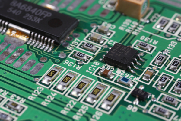
In the PCB industry, flat refers to a specific type of package used for surface-mount components on printed circuit boards. These packages are rectangular or square in shape and have leads positioned on opposite sides of the package. This design enables the gull wing leads to be easily surface mounted on the PCB.
The flat package is commonly used in conjunction with other package names, such as Ceramic FlatPack (or Flat Pack) and Quad Flat Pack (QFP). A Ceramic FlatPack is a hermetically sealed package made of ceramic material, primarily utilized in high reliability applications such as space, radiation, military, or defense. It can also find application in special commercial scenarios.
The military standard MIL-STD-1835C provides a precise definition for the flat package (FP). According to this standard, a flat package is a rectangular or square package with leads parallel to the base plane, attached on two opposing sides of the package periphery. The standard further outlines various types of flat packages, each with distinct parameters including package body material, terminal location, package outline, lead form, and terminal count.
The invention of the flat package can be attributed to Y. Tao in 1962 while working for Texas Instruments. It was developed as an improvement over the round TO-5 style transistor packages previously used for integrated circuits. The flat package offered advantages such as enhanced heat dissipation, smaller size, and the ability to provide hermetic seals for circuits using glass, ceramic, or metal materials.


