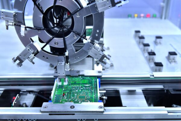
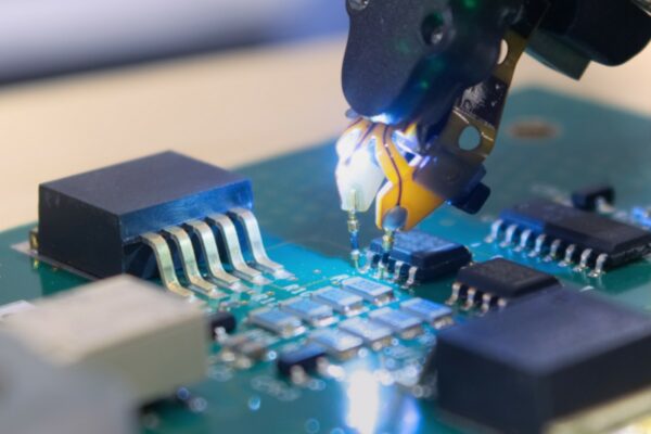
What is Fine Line Design
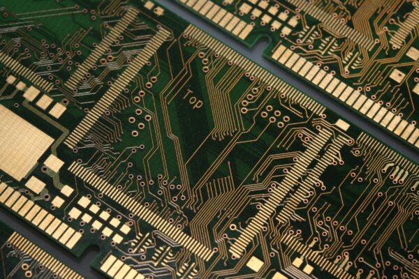
Fine line design is the specialized process of designing and manufacturing PCBs with extremely small line widths and spacing. These fine lines are typically around 0.004 inches or smaller in width, allowing for higher-density features and the accommodation of more components within a limited space.
Achieving fine line designs requires careful consideration of the selection of appropriate materials and processes. For instance, the use of premium dry film with enhanced clarity is often necessary to resolve images accurately when dealing with fine lines on both inner and outer layers of the PCB.
The imaging process is another factor. Traditional exposure units, which utilize a single point light source spread across the production panel using reflectors, may not be suitable for achieving the desired precision. The angle at which the light hits the panel can hinder fine line imaging. Therefore, it is essential to employ exposure units that minimize this issue and ensure optimal results.
Chemical etching, which removes unwanted material from the PCB, can potentially eat away a small amount of the masked material and result in broken lines if the lines are too narrow. Additionally, the risk of short circuits between closely spaced lines due to flexing or manufacturing imperfections must be carefully addressed.
