What is Fabrication
Fabrication, in the context of the PCB industry, refers to the stage of PCB development where the circuit board design is transformed into a physical structure. It encompasses a series of manufacturing steps that are essential in creating a functional printed circuit board.
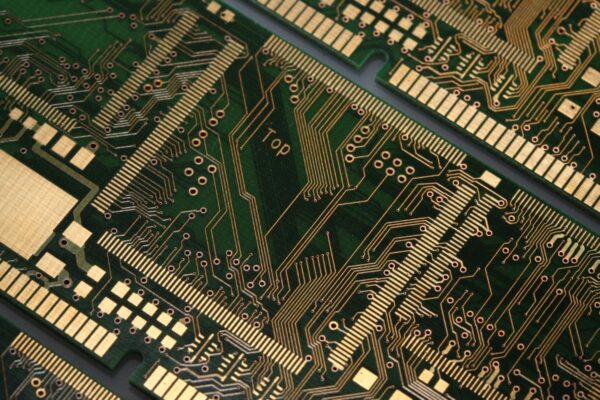
The fabrication process begins with imaging the layout onto the copper-clad laminate. This involves transferring the circuit pattern onto the copper surface using a photosensitive material or other imaging techniques. Once the desired layout is imaged, the excess copper is etched away, revealing the traces and pads. This selective removal of copper is achieved through the use of chemical etchants that dissolve the unwanted copper while preserving the desired circuit pattern.
After the inner layers are etched, the PCB layer stackup is created by laminating multiple layers of copper-clad laminates and insulating materials together. This process involves heating and pressing the materials to form a solid structure. Holes are then drilled in the PCB for mounting holes, through-hole pins, and vias, providing mechanical support and electrical connectivity between different layers.
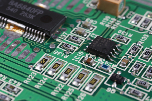
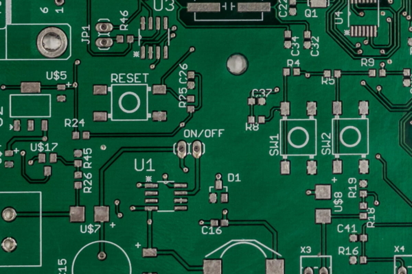
To ensure good electrical conductivity and mechanical strength, the pin holes and via holes are plated with a thin layer of metal, typically copper. This plating process creates a conductive pathway within the holes. Additionally, a protective coating or solder mask is applied to the surface of the PCB to prevent oxidation, corrosion, and solder bridging during assembly and operation. Silkscreen printing is also performed to add reference indicators, logos, or other markings on the surface, aiding in component placement and identification.
