What is DNP
In the PCB industry, DNP stands for “Do Not Place.” It is an abbreviation commonly used in PCB design to indicate that a specific component should not be populated or installed on the PCB during the manufacturing process. This designation provides several benefits in the design and manufacturing of PCBs.
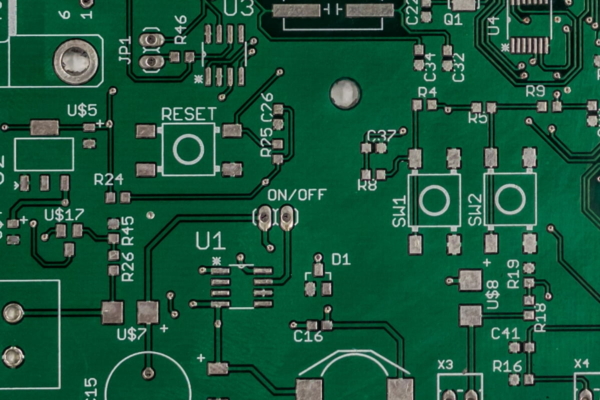
When a component is marked as DNP on a schematic or assembly drawing, it means that it is intentionally left unpopulated on the PCB. There are several reasons for using the DNP designation. Firstly, it allows for cost optimization by excluding components that may not be required or add unnecessary cost during the initial production run. Secondly, it provides design flexibility, allowing the designer to easily modify the PCB assembly without redesigning the entire board. This can be particularly useful when there is a need for customization or specific requirements.
Additionally, the DNP designation aids in testing and debugging during the prototyping phase. By marking certain components as DNP, the designer can isolate specific sections of the circuit or replace components for troubleshooting purposes. Lastly, the DNP designation can be used to indicate alternate component selection, providing the option to use different components with varying specifications or characteristics.
DNP designation is typically used during the schematic design phase and is carried forward to the PCB layout. The manufacturing instructions provided to the PCB manufacturer will specify that the components marked as DNP should not be populated on the final board.
