What is Copper Pour
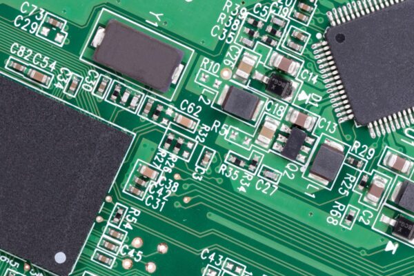
Copper pour, also known as copper pouring, describes an area on a PCB layer that is filled with copper. This copper-filled area can be located on the top, bottom, or any internal layer of the PCB stack-up. A copper pour creates a conductive surface for making connections in the PCB.
Copper pour can create a ground plane. A ground plane is a layer of copper that exists on a different layer or electrical net from the other components and is connected to them only as a grounding material. This allows the electricity in the PCB to be grounded into the copper pour, providing a common point of reference for determining voltage. The copper pour also helps in reducing the amount of etching fluid used during PCB manufacturing.
In addition to its use as a ground plane, a copper pour can also be used for thermal dissipation. Copper is not only highly conductive electrically but also has high thermal conductivity. By incorporating vias, the copper pour can help dissipate heat generated by components or circuitry on the PCB, preventing overheating issues and improving overall thermal management.
