What is Conductive Pattern
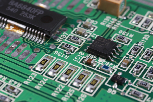
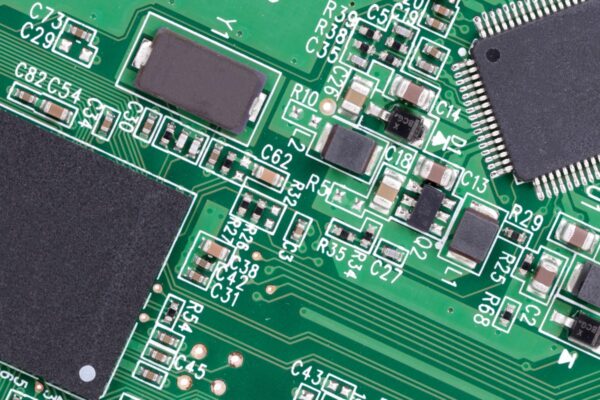
A conductive pattern, in the context of the PCB, refers to the specific configuration or design of the conductive material on a printed circuit board (PCB) that allows for the flow of electrical energy. This pattern is formed by selectively depositing a conductive material, typically copper, onto the PCB surface using a resist material to prevent plating in undesired areas.
The conductive pattern encompasses various elements, including conductors, lands, and through connections, which collectively make up the circuit on the PCB. These elements are responsible for connecting different electronic components and circuitry on the board, enabling the flow of electrical current and the transmission of signals.
To create the conductive pattern, a process called pattern plating is employed. This involves selectively plating the conductive material onto the PCB to form the desired pattern. The selective plating process ensures that the conductive material is deposited only in the areas where it is intended, while the resist material prevents plating in other areas.
Conductive pattern is very important for the functionality of the PCB and the electronic devices it is used in. It provides the necessary electrical connections between components, allowing for the proper operation of the circuit. By defining the pathways for current flow, the conductive pattern enables the efficient transmission of signals and the overall functionality of the PCB.
