Clearance Definition
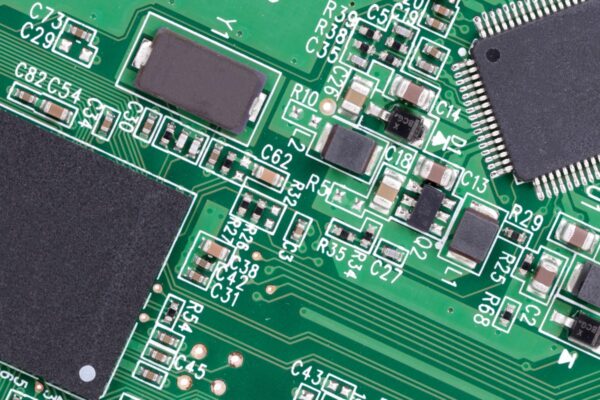
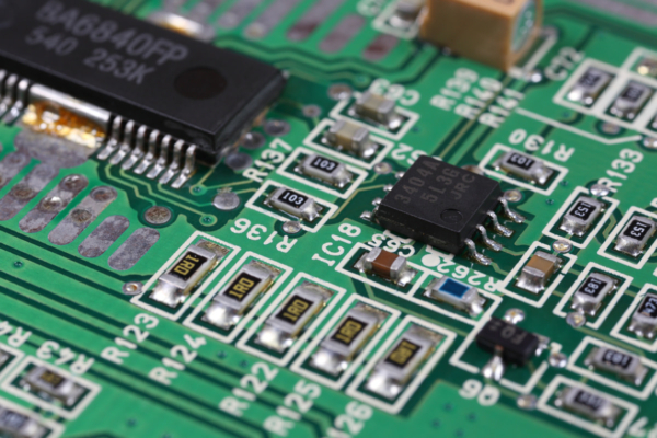
Clearance in the PCB industry refers to the minimum distance between any two conductors or between a conductor and the edge of the PCB board. It is a critical design aspect that relates to safety, noise suppression, and manufacturability. The clearance values are determined based on the voltage and frequency of the signals, and they need to be balanced with crosstalk suppression guidelines to ensure signal integrity. Clearance values are encoded as design rules in ECAD software.
Frequently Asked Questions
What is PCB creepage and clearance?
Creepage pertains to the separation between two conductors on the board’s surface or along the insulating material’s surface. On the other hand, clearance refers to the direct distance between two conductors through the air, without any obstructions.
Why is creepage and clearance important?
Adequate measurement of clearance and creepage distance is necessary to safeguard individuals or systems from the impact of electrical operating voltages, particularly in the event of equipment malfunction.
What is the 3W rule in PCB?
To minimize coupling between parallel traces, the 3W rule for crosstalk suggests that they should be separated by a distance of at least 3 times the width of the trace, measured from center to center. Here, W refers to the width of the trace.
What is clearance standard?
The definition of clearance standard refers to the highest allowable level of asbestos fibers in the air of an asbestos work area after the completion of asbestos abatement.
What is the clearance for 100V PCB?
To ensure safe operation of a trace carrying 100V, a separation of 0.1 mm is necessary. Additionally, it is important to take into account the Comparative Tracking Index (CTI) of the PCB being utilized.
What is the clearance distance?
The clearance distance refers to the minimum distance between two conductive parts or between a conductive part and the bounding surface of the equipment, which is measured through air. This distance is crucial in preventing dielectric breakdown between electrodes that can be caused by the ionization of air.
How much clearance do you need for a PCB hole?
To avoid any issues, it is recommended to maintain a minimum distance of 0.010″ between the board edge and both plated and unplated drilled holes. It is important to consider other PCB drill rules in addition to the minimum edge clearance. Furthermore, it is advisable to keep copper traces and planes at least 0.010″ away from the PCB edge.
What is a good amount of clearance?
In general, a vehicle that has a clearance of 8.5 inches or higher is considered to be suitable.
What are the three levels of clearance?
The security clearance system comprises of three levels: confidential, secret, and top secret.
What is the UL standard for PCB?
The safety and testing standard for printed wiring boards is known as UL 796, which is followed by Sierra for all their circuit board production. Additionally, CAN/CSA-C22 is also considered for this purpose.
What are the standards for creepage?
For basic insulation, a minimum creepage of 2.5 mm is required. However, for reinforced insulation, the distance must be twice as long as basic insulation, which means that the creepage for reinforced insulation should be at least 5.0 mm.
How close can components be on a PCB?
It is recommended to maintain a minimum distance of 40mil between the components and a minimum distance of 100mil between each component and the edge of the PCB. Additionally, it is advisable to avoid placing components near through-hole terminals on the solder side of the PCB.
Is clearance the same as tolerance?
The definition of tolerance refers to the range of acceptable measurements for a part, including its length, width, or diameter. On the other hand, clearance pertains to the space or gap between two parts that fit together, such as a hole and a shaft.
What is maximum clearance vs minimum clearance?
To avoid plagiarism, here’s a possible rewrite of the given text while keeping the original meaning: Text: Clearance Limits
The maximum clearance limit for a fit refers to the gap between the highest diameter of the orifice and the lowest diameter of the shaft. On the other hand, the minimum clearance limit is the gap between the lowest diameter of the orifice and the highest diameter of the shaft.
What is clearance in measuring?
Clearance is a pharmacokinetic parameter that measures the amount of plasma from which a substance is entirely eliminated per unit time in pharmacology. Typically, clearance is expressed in L/h or mL/min and indicates the rate of drug elimination divided by plasma concentration.
What is the clearance of PCB components?
In order to prevent any harm to the cutting tools, it is recommended to position the components at a distance of 0.050 to 0.075 inches from the board’s edge. For taller components like electrolytic capacitors, it is advisable to set them back 0.125 inches from the board’s edge.
What is the standard PCB hole distance?
The usual distance between the center of two holes on a PCB is typically at least 0.100 inches, even for DIP processors. This ample spacing facilitates manual soldering of through-hole PCBs.
What is the 5H rule in PCB?
It is recommended to maintain a minimum distance of 5H between the void and the edge of a trace, as well as between the edge of a trace and the reference plane in the open field region.
What is 20h rule in PCB design?
The 20-H rule refers to a guideline for designing printed circuit board layouts. Its purpose is to contain the fringing field at the edges of the board, particularly on boards that have power and ground planes. This is achieved by ensuring that the edge of the power plane is backed away from the edge of the board by a distance that is equivalent to 20 times the separation distance between the planes.


