What is Bridging
Bridging, in the context of the PCB industry, refers to a defect that occurs during the soldering process. It happens when an excessive amount of solder is applied, causing two or more pads on the PCB to form an unintended connection or “bridge” between them. This bridge creates an unintended electrical pathway, which can lead to various issues such as trace damage, component damage, or even short circuits.
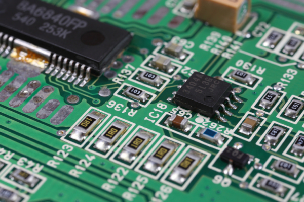
The miniaturization of electronic devices has increased the need to fit more components into smaller package sizes. As a result, the density of components on PCBs has increased, making them more prone to manufacturing issues like solder bridging. When components are placed closer together, there is a higher chance of solder flowing between adjacent pads, creating unintended electrical connections.
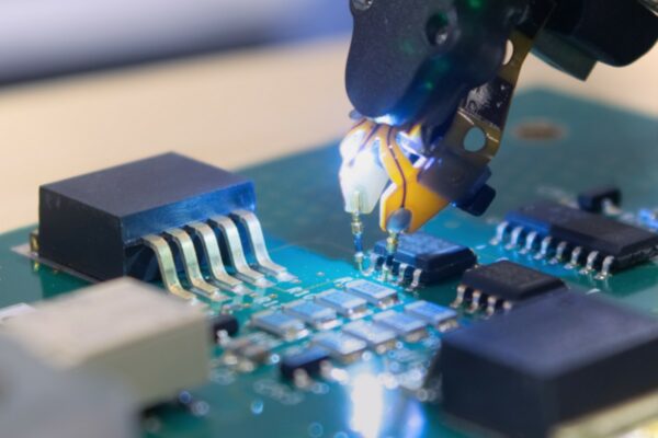
Detecting solder bridging can be challenging as the bridges formed by excessive solder may not be easily visible to the naked eye. Specialized equipment or techniques, such as optical inspection, may be required to identify and diagnose solder bridging accurately.
To prevent excessive solder application and minimize the risk of bridging, a solder mask can be applied during the PCB fabrication process. A solder mask is a solder-resistant coating that is added to the PCB. It selectively covers certain areas, preventing solder from being applied to those regions during the soldering process. This helps ensure that solder is applied only where intended, reducing the likelihood of bridging.
Frequently Asked Questions
What Happens if You Create a Solder Bridge on Your PCB
Bridge soldering occurs when excessive solder causes two or more component pads to connect on a PCB. This unintended electrical connection can lead to various issues and disruptions.
