What is Automatic Component Placement
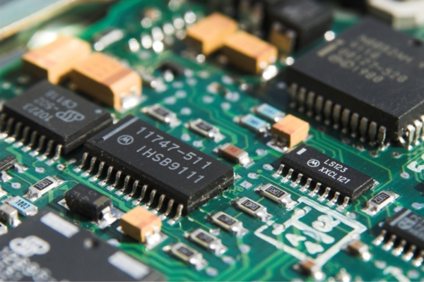
Automatic Component Placement, in the context of the PCB industry, refers to a method or feature in PCB design software that automates the arrangement and positioning of components on a printed circuit board (PCB). This process is based on the netlist imported from the schematic and aims to optimize the placement of components by considering various factors such as the physical realization of the circuit, packaging constraints, and the proximity of components in the schematic.
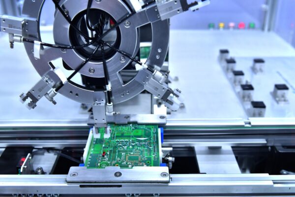
Automatic component placement streamlines the PCB design process and improves the efficiency of assembly. By automatically aligning similar components in the same direction, it facilitates effective routing and ensures error-free soldering during assembly. This not only reduces downtime and turnaround time in PCB manufacturing but also enhances the performance and reliability of the final product.
While automatic component placement can assist in the initial organization of footprints on the PCB, it may not always result in an optimized PCB layout. The effectiveness of this method may vary depending on the complexity of the circuit and the specific requirements of the design. Designers should also consider other factors such as clearance and spacing rules, standardized component orientation, and the allocation of space for copper traces to ensure a robust and reliable design.
