What is Artwork Master
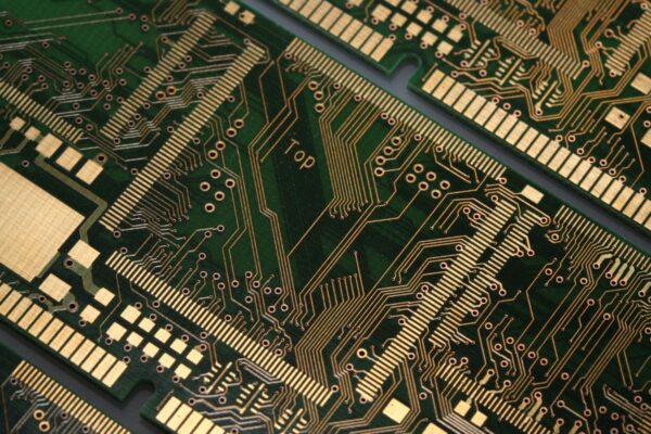
An artwork master is a photographic film or glass plate that embodies the image of the PCB pattern, typically on a 1:1 scale. This image serves as a template for creating the actual circuit board. It contains the precise layout and design of the circuitry, including the placement of components, traces, and vias. Any errors or inaccuracies in the Artwork Master can result in faulty PCBs, leading to potential electrical failures or performance issues.
To create the artwork master, a photolithography process is employed. It begins with a design file, which is then converted into a photographic image on a film or glass plate. This image represents the desired pattern of the PCB and is used to transfer the pattern onto the PCB substrate during the manufacturing process.
The 1:1 scale of the artwork master ensures that the pattern is accurately reproduced on the PCB, maintaining the integrity and functionality of the circuit. It serves as a reference for all subsequent manufacturing steps, including the creation of the photomask, which is used to transfer the pattern onto the PCB substrate.
