Printed circuit boards (PCBs) are the backbone of modern electronics, providing a platform for interconnecting and supporting various components. These unsung heroes can be found in almost every electronic device we use daily, from smartphones and computers to medical equipment and automotive systems. But have you ever wondered what materials go into making these essential components?
In this article, we’ll dive deep into the world of PCB materials, exploring the key components that make up these intricate boards and how their properties influence the performance and reliability of electronic devices.
Introduction to PCB Materials
A printed circuit board is a flat, rigid structure that contains electrical circuitry made up of embedded metal surfaces called traces and larger areas of metal called planes. Components are soldered to the board onto metal pads, which are connected to the board circuitry, allowing them to be interconnected. A PCB can be composed of one, two, or multiple layers of circuitry.
PCBs are built with a dielectric core material that has poor electrical conducting properties to ensure pure circuitry transmission. This core is interspaced with extra layers of metal and dielectric as needed. The standard dielectric material used for circuit boards is a flame-resistant composite of woven fiberglass cloth and epoxy resin, known as FR-4, while the metal traces and planes for the circuitry are usually composed of copper.
The key components of a PCB include:
- Substrate: Provides mechanical support and electrical insulation
- Conductive layer: Usually copper, forms the circuit paths
- Solder mask: Protective layer that insulates and prevents solder bridges
- Silkscreen: Adds text and symbols for identification
The choice of materials for each of these components affects the PCB’s performance, durability, and cost. Understanding the properties and characteristics of these materials is crucial for designing and manufacturing reliable and efficient electronic devices.
Substrate Materials
The substrate is the foundation of a PCB, providing mechanical support and electrical insulation for the conductive layers. It is typically made from a dielectric material, which has poor electrical conducting properties to ensure pure circuitry transmission. The most common substrate material used in PCBs is FR-4, a flame-resistant composite of woven fiberglass cloth and epoxy resin.
FR-4 is widely used due to its excellent properties, including:
- High strength-to-weight ratio
- Good electrical insulation
- Flame retardance
- Moisture resistance
- Relative temperature resistance (typically rated for 50°C to 115°C)
FR-4 substrates come in various grades, each with specific properties tailored to different applications. For example, high-temperature FR-4 (high Tg) is compatible with lead-free reflow technology and can withstand temperatures up to 170°C to 180°C. Halogen-free FR-4 is another variant that complies with environmental regulations and is compatible with lead-free reflow technology.
In addition to FR-4, other substrate materials are used in PCBs for specific applications:
- Rogers: Polymer-ceramic composites that offer high thermal stability and good electrical performance, making them suitable for high-frequency and high-performance circuits.
- Polyimide: A flexible, heat-resistant material used in flexible PCBs and high-temperature environments.
- Metal-core (e.g., aluminum): Provides improved thermal management and is used in high-power electronics and LED lighting applications.
When choosing a substrate material, engineers must consider factors such as electrical properties, thermal properties, and cost. The right substrate material ensures that the PCB can meet the specific requirements of the application while maintaining reliability and performance.
Conductive Materials
Conductive materials play a crucial role in PCBs, forming the circuit paths that allow electrical signals to travel between components. The most commonly used conductive material in PCBs is copper, thanks to its excellent conductivity and cost-effectiveness.
Copper thickness is an important consideration in PCB design, as it affects the current-carrying capacity and signal integrity of the traces. Copper thickness is typically measured in ounces per square foot (oz/ft²), with 1 oz/ft² being the most common thickness. This translates to approximately 35 µm or 1.4 mils. Thicker copper layers, such as 2 oz/ft² or 3 oz/ft², are used in high-power applications or when greater mechanical strength is required.
While copper is the primary conductive material in PCBs, other materials are sometimes used for specific applications:
- Aluminum: Used in some high-power applications due to its lower cost and weight compared to copper.
- Silver and Gold: Used in specialized applications or as plating to improve conductivity and corrosion resistance.
To protect copper traces from oxidation and ensure reliable soldering, they are often coated with a protective layer, such as a solder mask or gold plating. The solder mask also helps to prevent solder bridges between closely spaced pads during the assembly process.
Another important consideration in PCB design is the width of the copper traces. The trace width directly affects the current-carrying capacity of the circuit, with wider traces being able to handle higher currents. However, increasing trace width also increases the overall size of the PCB, so designers must strike a balance between current-carrying capacity and board size.
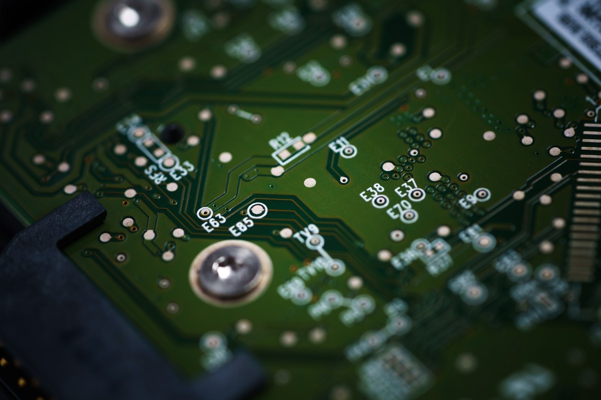
Solder Mask
Solder mask, also known as solder resist or solder stop mask, is a thin, protective layer of polymer applied to the copper traces of a PCB. Its primary purpose is to insulate the conductive traces and prevent accidental short circuits during the soldering process.
Solder mask is typically composed of an epoxy-based polymer that is applied to the PCB surface using screen printing or liquid photo imaging (LPI) techniques. After application, the solder mask is cured using heat or ultraviolet (UV) light to create a durable, protective layer.
The most common color for solder mask is green, but other colors, such as blue, red, and black, are also available. Green is the most popular choice because it provides good contrast against the copper traces and makes it easier to inspect the PCB for defects.
The main functions of solder mask include:
- Preventing solder bridges: By covering the spaces between copper traces, solder mask prevents accidental solder connections that can cause short circuits.
- Protecting copper traces: Solder mask shields the copper traces from environmental factors, such as moisture and dust, which can cause corrosion and deterioration over time.
- Providing electrical insulation: The solder mask acts as an insulating layer, preventing electrical contact between adjacent traces and components.
The typical thickness of a solder mask layer ranges from 0.8 to 1.0 mils (20 to 25 µm). The thickness is carefully controlled to ensure that the mask provides adequate protection without interfering with the soldering process or the placement of components.
Solder mask plays a critical role in the overall PCB manufacturing process, ensuring the reliability and longevity of the finished product. Without a properly applied solder mask, PCBs would be more susceptible to short circuits, corrosion, and other issues that could compromise their performance and lifespan.
Silkscreen
Silkscreen, also known as legend or nomenclature, is a layer of text and symbols printed on the surface of a PCB to provide important information for assembly, testing, and troubleshooting. Unlike the solder mask, which serves a functional purpose, the silkscreen is primarily used for identification and communication.
The silkscreen is typically printed using an epoxy-based, heat-resistant ink that adheres well to the PCB surface. The most common color for silkscreen is white, as it provides excellent contrast against the darker solder mask. However, other colors, such as yellow, can also be used.
The information included in the silkscreen can vary depending on the specific requirements of the PCB, but it often includes:
- Component designators: Labels that identify the location and type of each component on the board, such as “R1” for a resistor or “C2” for a capacitor.
- Reference designators: Unique identifiers for each component that correspond to their schematic symbol and bill of materials (BOM) entry.
- Polarity indicators: Symbols that show the correct orientation of polarized components, such as electrolytic capacitors and diodes.
- Manufacturer logos: Branding elements that identify the PCB manufacturer or the company that designed the board.
- Warning symbols: Safety-related information, such as high-voltage warnings or ESD-sensitive device handling instructions.
The silkscreen is applied to the PCB using either screen printing or inkjet printing techniques. Screen printing involves using a stencil to transfer the ink onto the PCB surface, while inkjet printing uses a digital printer to deposit the ink directly onto the board.
The presence of a clear and accurate silkscreen is crucial for PCB assembly and troubleshooting. It helps technicians quickly identify components and their proper placement, reducing the risk of assembly errors and making it easier to diagnose and repair issues that may arise during the product’s lifetime.
Types of PCBs and Material Considerations
PCBs come in various types, each with its own unique structure and material requirements. The three main categories of PCBs are single-sided, double-sided, and multi-layer boards. The choice of materials for each type depends on factors such as the complexity of the circuit, the operating environment, and the desired performance characteristics.
Single-Sided PCBs
Single-sided PCBs have conductive material on only one side of the substrate. They are the simplest and most cost-effective type of PCB, making them suitable for basic, low-density circuits. The most common substrate material for single-sided PCBs is FR-4, while the conductive layer is typically made of copper.
Single-sided PCBs are often used in consumer electronics, such as toys and simple appliances, where cost is a primary concern. However, their limited routing options and lower component density make them less suitable for more complex designs.
Double-Sided PCBs
Double-sided PCBs have conductive material on both sides of the substrate, allowing for more complex circuits and higher component density. These boards often incorporate through-holes and vias to connect the conductive layers on opposite sides.
The material considerations for double-sided PCBs are similar to those for single-sided boards, with FR-4 being the most common substrate material. However, the increased complexity of double-sided designs may require the use of higher-grade materials or specialized substrates to ensure proper performance and reliability.
Double-sided PCBs are used in a wide range of applications, including consumer electronics, industrial controls, and telecommunications equipment.
Multi-Layer PCBs
Multi-layer PCBs consist of three or more conductive layers separated by insulating layers. These boards offer the highest component density and routing options, making them suitable for complex, high-performance applications.
The material selection for multi-layer PCBs is critical, as the increased number of layers and the close proximity of the conductive traces can lead to signal integrity issues, such as crosstalk and electromagnetic interference (EMI). To mitigate these issues, designers may use specialized substrate materials with low dielectric constants and dissipation factors, such as Rogers or Isola materials.
In addition to signal integrity concerns, multi-layer PCBs also face challenges related to thermal management and mechanical stress. The use of high-performance materials, such as polyimide or ceramic substrates, can help address these issues and ensure reliable operation in demanding environments.
Multi-layer PCBs are commonly found in high-performance applications, such as aerospace, defense, and medical equipment, where reliability and performance are paramount.
The choice of materials for each type of PCB has a significant impact on the board’s performance, cost, and manufacturing complexity. By carefully selecting the appropriate materials based on the specific requirements of the application, designers can ensure that their PCBs meet the necessary performance and reliability standards while minimizing costs and production challenges.
Conclusion
In conclusion, the materials used in the construction of printed circuit boards play a crucial role in determining the performance, reliability, and cost of electronic devices. The four key components of a PCB – substrate, conductive materials, solder mask, and silkscreen – each serve a specific purpose and contribute to the overall functionality of the board.
The substrate, typically made of FR-4 or other specialized materials, provides the foundation for the PCB, offering mechanical support and electrical insulation. Conductive materials, primarily copper, form the circuit paths that allow electrical signals to flow between components. The solder mask protects the copper traces from damage and prevents short circuits during the soldering process, while the silkscreen provides essential information for assembly and troubleshooting.
As technology advances and the demand for high-performance electronics grows, new trends in PCB materials are emerging. Environmentally friendly options, such as halogen-free substrates and lead-free solders, are becoming increasingly popular as manufacturers strive to reduce their ecological footprint. Additionally, the development of advanced materials, such as low-loss substrates and high-frequency laminates, is enabling the design of PCBs that can operate at higher frequencies and support the latest communication standards.
For engineers and designers, a deep understanding of PCB materials is essential for creating effective and efficient electronic devices. By carefully selecting the appropriate materials based on the specific requirements of the application, designers can optimize the performance, reliability, and cost of their products. As the electronics industry continues to evolve, staying up-to-date with the latest advancements in PCB materials will be crucial for success in this dynamic and innovative field.


 Circuit Board Assembly")


 PCB Technology: Types, Benefits, Challenges, and Applications")