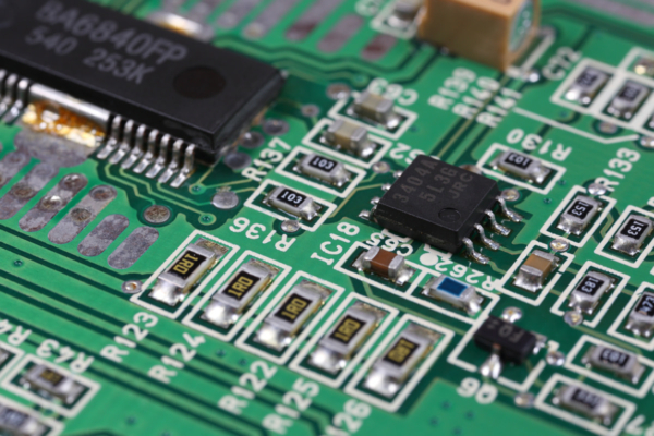
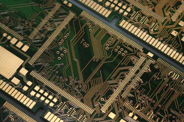
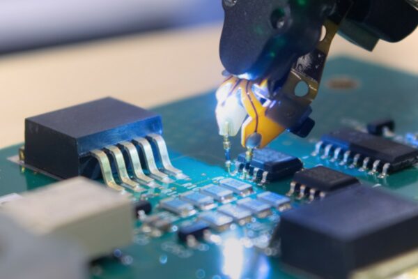
The landscape of electronics manufacturing has undergone a profound transformation in recent decades, largely driven by the advent and widespread adoption of Surface Mount Technology (SMT). To truly appreciate the significance of SMT, one must consider the limitations of its predecessor, through-hole technology. Through-hole, with its component leads inserted into drilled holes and soldered on the opposite side of the board, imposed constraints on component density and miniaturization. The emergence of SMT in the 1980s marked a paradigm shift, enabling the placement of components directly onto the surface of printed circuit boards (PCBs). This seemingly simple change had far-reaching consequences, paving the way for smaller, lighter, and more sophisticated electronic devices.
A Historical Perspective: From Through-Hole to SMT
The journey from through-hole to SMT was not an overnight revolution but rather a gradual evolution driven by the relentless pursuit of miniaturization and increased functionality. Early SMT processes faced challenges related to component availability, equipment maturity, and process reliability. However, the inherent advantages of SMT, such as reduced board size, improved electrical performance, and suitability for automation, quickly became apparent. Pioneers in industries like consumer electronics and telecommunications embraced SMT, driving innovation in equipment, materials, and process development. Each incremental improvement built upon the last, leading to the sophisticated SMT ecosystem we have today.
The Fundamental Shift: Miniaturization and Increased Functionality
The core advantage of SMT lies in its ability to facilitate the use of smaller components and achieve higher component densities on PCBs. This miniaturization is not merely about shrinking physical dimensions; it’s about packing more functionality into a given space. SMT allows for the placement of components on both sides of the board, effectively doubling the available real estate. Moreover, the shorter leads and smaller package sizes of SMT components result in reduced inductance and capacitance, leading to improved signal integrity and faster operating speeds. This is particularly crucial in high-frequency applications, where signal integrity is paramount.
SMT’s Impact Across Industries: A Brief Overview
The impact of SMT is pervasive, touching virtually every industry that relies on electronics. In consumer electronics, SMT has enabled the development of smartphones, tablets, laptops, and countless other portable devices. The automotive industry leverages SMT for engine control units, infotainment systems, and advanced driver-assistance systems (ADAS), where reliability under harsh conditions is critical. In aerospace, SMT’s ability to reduce weight and improve performance is paramount. Medical device manufacturers rely on SMT for miniaturized implantable devices, diagnostic equipment, and patient monitoring systems. Industrial automation benefits from SMT’s robustness and ability to withstand harsh environments. This brief overview merely scratches the surface; the applications of SMT are as diverse as the industries that employ them.
Core Principles of SMT Assembly: A Detailed Examination
The SMT assembly process, at its core, is a symphony of precision and automation. Each step, from component placement to reflow soldering, plays a critical role in ensuring the quality and reliability of the final product. A deep understanding of these processes requires delving into the intricacies of each stage.
Component Placement: Precision and Automation
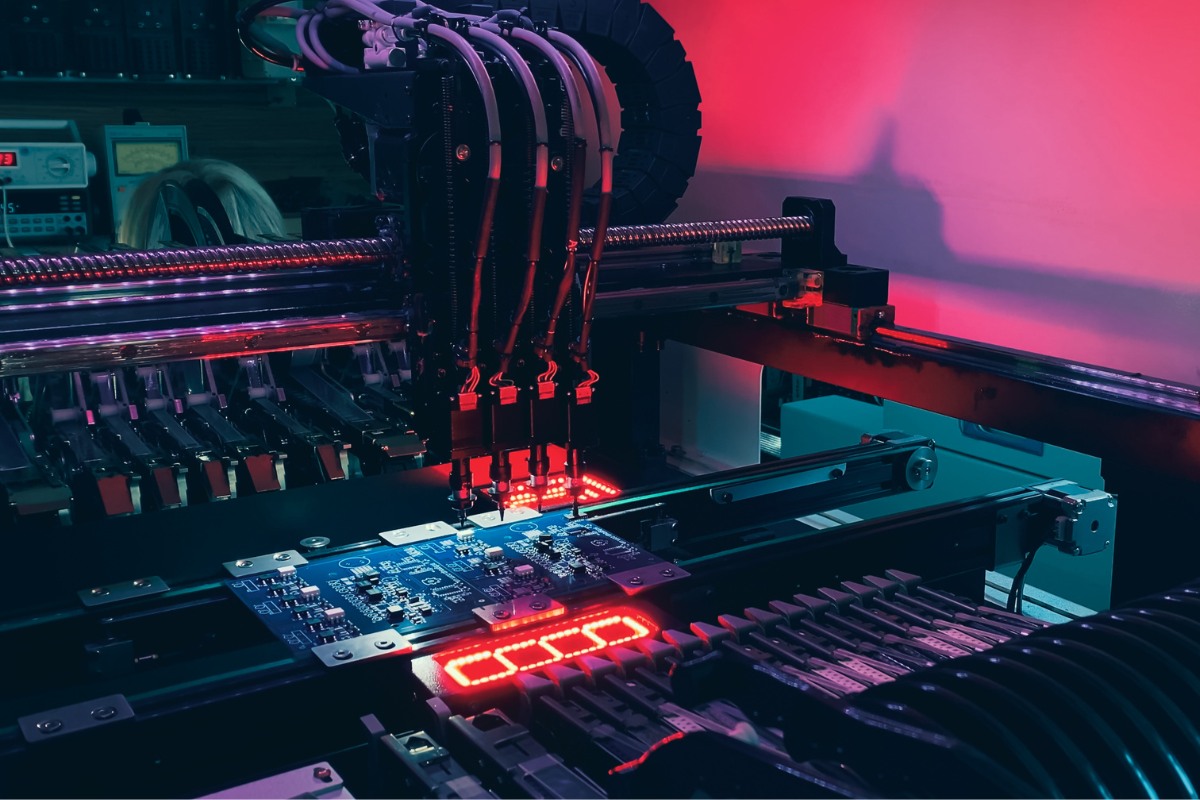
The accurate placement of components on the PCB is the cornerstone of SMT assembly. This task is entrusted to sophisticated pick-and-place machines, marvels of engineering that combine speed, precision, and flexibility.
Pick-and-Place Machines: Types, Capabilities, and Limitations
Pick-and-place machines come in various configurations, each tailored to specific needs. “Chip shooters” are optimized for high-speed placement of small, passive components, while “flexible placers” handle a wider range of component sizes and shapes, including integrated circuits (ICs). Modular systems offer scalability, allowing manufacturers to add placement heads as needed. These machines boast impressive placement rates, often exceeding tens of thousands of components per hour. However, accuracy is paramount. Modern machines achieve placement accuracy down to a few tens of micrometers, but this is constantly challenged by the ever-decreasing size of components. Factors like machine calibration, component centering mechanisms, and the inherent stability of the machine itself all contribute to placement accuracy. Even the slightest vibration or misalignment can lead to defects.
Vision Systems and Fiducial Recognition: Ensuring Accuracy
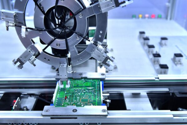
To achieve the required precision, pick-and-place machines rely heavily on advanced vision systems. These systems use high-resolution cameras and sophisticated algorithms to locate and orient components and to register the PCB accurately. Fiducial markers, small, precisely defined patterns placed on the PCB, serve as reference points for the vision system. The machine uses these fiducials to compensate for any minor misalignments or distortions in the board. Different types of fiducials exist, including global fiducials for overall board registration and local fiducials for fine-pitch component alignment. The accuracy of the vision system is influenced by factors such as lighting conditions, the contrast between the fiducial and the board surface, and the sophistication of the image processing algorithms.
Component Feeders: Optimizing for Speed and Reliability
Component feeders are the unsung heroes of the pick-and-place process, responsible for delivering components to the placement head in a precise and timely manner. Tape and reel feeders are the most common, housing components in individual pockets within a carrier tape. Tray feeders are used for larger components or those that are not suitable for tape and reel packaging. Tube feeders are employed for components with specific orientation requirements. Intelligent feeders, equipped with sensors and communication capabilities, can provide real-time feedback on component availability and feeding status, minimizing downtime and preventing errors. The design and maintenance of feeders are critical to ensuring reliable component feeding, especially for very small or delicate components.
Solder Paste Application: The Critical Foundation
Solder paste application is a critical step that lays the foundation for reliable solder joints. The precise deposition of solder paste onto the PCB pads ensures that the right amount of solder is available for each connection.
Stencil Printing: Process Parameters and Material Considerations
Stencil printing is the most widely used method for solder paste application. A thin, stainless steel or nickel stencil with apertures corresponding to the PCB pads is aligned over the board. Solder paste is then forced through the apertures using a squeegee, depositing a precise amount of paste onto each pad. The stencil printing process is highly sensitive to various parameters, including squeegee pressure, speed, and angle. These parameters must be carefully controlled to ensure consistent paste deposition and prevent defects. Stencil thickness and aperture design are also crucial. The thickness determines the volume of paste deposited, while the aperture shape and size influence the paste release characteristics. Advanced stencil technologies, such as step stencils (with varying thicknesses across the stencil) and electroformed stencils (with smoother aperture walls), are employed to address the challenges of fine-pitch and complex component assembly.
Solder Paste Composition: Rheology, Flux, and Particle Size
Solder paste is a complex material, a carefully formulated mixture of solder alloy powder, flux, and other additives. The rheology of the paste, its flow characteristics under stress, is critical for successful stencil printing. The paste must be viscous enough to retain its shape after printing but also flow readily through the stencil apertures. Flux plays a vital role in removing oxides from the component leads and PCB pads, promoting wetting and ensuring a strong metallurgical bond. The type of flux used depends on the specific application and the required cleaning process. Solder particle size distribution also influences paste performance. Smaller particles offer better print definition for fine-pitch applications but can be more prone to oxidation. The choice of solder paste is a critical decision, impacting both the assembly process and the long-term reliability of the product.
Common Defects: Bridging, Tombstoning, and Voids
Despite meticulous process control, solder paste printing defects can occur. Bridging, the unwanted connection between adjacent pads, is often caused by excessive paste deposition or poor stencil alignment. Tombstoning, where a component stands up on one end during reflow, can result from uneven paste deposition or imbalances in surface tension. Voids, or air pockets within the solder joint, can compromise the mechanical strength and thermal conductivity of the connection. These defects can arise from various factors, including improper stencil design, incorrect printing parameters, and suboptimal solder paste properties. Detecting and preventing these defects requires a thorough understanding of the underlying causes and the implementation of appropriate corrective actions.
Reflow Soldering: The Art and Science of Thermal Profiles
Reflow soldering is the process of heating the solder paste to melt the solder alloy, forming a permanent metallurgical bond between the component leads and the PCB pads. This seemingly simple process is, in fact, a complex interplay of heat transfer, material science, and precise temperature control.
Convection Reflow: Heat Transfer Mechanisms and Zone Control
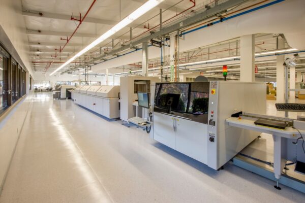
Convection reflow ovens are the workhorses of SMT assembly, utilizing forced hot air to heat the PCB and its components. These ovens are typically divided into multiple zones, each with independent temperature control. The PCB travels through the oven on a conveyor belt, experiencing a carefully orchestrated thermal profile. The profile typically consists of four distinct zones: preheat, soak, reflow, and cooling. The preheat zone gradually raises the temperature of the board and components, activating the flux and minimizing thermal shock. The soak zone allows the temperature to equalize across the board, ensuring uniform heating. The reflow zone elevates the temperature above the solder’s melting point, forming the solder joints. Finally, the cooling zone solidifies the solder joints, controlling the cooling rate to minimize stress and optimize the microstructure of the solder. Achieving the optimal thermal profile is a delicate balancing act, requiring careful consideration of the specific components, PCB materials, and solder paste used.
Vapor Phase Reflow: Advantages and Limitations in Specific Applications
Vapor phase reflow offers an alternative to convection heating, utilizing the latent heat of vaporization of a specialized fluid to transfer heat to the PCB. The assembly is immersed in a saturated vapor, which condenses on the cooler surfaces, providing uniform and efficient heating. Vapor phase reflow is particularly advantageous for assemblies with high thermal mass or complex geometries, as it ensures excellent temperature uniformity regardless of component size or placement. It also minimizes oxidation due to the inert vapor environment. However, vapor phase reflow has limitations, including higher equipment and fluid costs, the need for specialized fluids with specific boiling points, and potential for component damage due to rapid heating. Consequently, it is typically used in niche applications where its unique benefits outweigh the drawbacks.
Nitrogen Atmosphere Reflow: Minimizing Oxidation and Enhancing Wetting
Reflow soldering in a nitrogen atmosphere has gained popularity due to its ability to minimize oxidation and improve solder wetting. By replacing the oxygen in the reflow oven with nitrogen, the formation of oxides on the component leads and PCB pads is significantly reduced. This results in cleaner solder joints with improved appearance and potentially enhanced reliability. Nitrogen also influences the surface tension of the molten solder, promoting better wetting and reducing the risk of defects like tombstoning and bridging. The purity level of the nitrogen is a critical factor, with higher purity levels generally yielding better results. While nitrogen reflow adds complexity and cost to the process, the benefits in terms of improved solder joint quality and reduced rework often justify the investment, particularly for high-reliability applications.
Post-Reflow Inspection and Testing: Ensuring Quality and Reliability
The final step in the SMT assembly process is a rigorous inspection and testing regime to ensure the quality and reliability of the assembled boards. This involves a combination of automated optical inspection, X-ray inspection, and electrical testing.
Automated Optical Inspection (AOI): Defect Detection and Classification
Automated Optical Inspection (AOI) systems are sophisticated vision systems that automatically inspect assembled PCBs for a wide range of defects. These systems use high-resolution cameras and advanced image processing algorithms to detect missing components, misalignment, solder bridges, insufficient solder, and other common defects. Different AOI techniques are employed, including template matching (comparing the image to a known good image), pattern recognition (identifying specific features or patterns), and statistical process control (analyzing variations in the image data). The effectiveness of AOI depends on factors such as lighting conditions, camera resolution, and the sophistication of the inspection algorithms. While AOI is highly effective in detecting surface-level defects, it cannot identify hidden defects within solder joints or under components.
X-ray Inspection: Unveiling Hidden Solder Joint Integrity
X-ray inspection provides a crucial window into the internal structure of solder joints, revealing hidden defects that are not visible to optical inspection. X-ray systems generate images based on the differential absorption of X-rays by different materials. Solder, being denser than most other materials on the PCB, absorbs more X-rays and appears darker in the image. This allows for the detection of voids, cracks, insufficient solder, and misalignment within solder joints, particularly for components like Ball Grid Arrays (BGAs) where the connections are hidden beneath the package. Different X-ray techniques exist, including 2D (providing a single projection image), 3D (creating multiple projection images from different angles), and computed tomography (CT), which generates cross-sectional images of the assembly. The choice of technique depends on the specific inspection requirements and the complexity of the assembly.
In-Circuit Testing (ICT) and Functional Testing: Validating Performance
In-Circuit Testing (ICT) and functional testing are electrical tests that verify the electrical connectivity and functionality of the assembled PCB. ICT typically uses a “bed of nails” fixture, a platform with an array of spring-loaded probes that make contact with specific test points on the board. This allows for the measurement of individual component values and the detection of shorts, opens, and other electrical defects. Functional testing, on the other hand, verifies the overall performance of the assembled board by simulating its intended operating environment and applying various input signals. This ensures that the board meets its specified functional requirements. The development of comprehensive test programs and the design of appropriate test fixtures are critical for effective ICT and functional testing.
Materials Science in SMT: A Deeper Look
The reliability and performance of SMT assemblies are intrinsically linked to the materials used in their construction. From the PCB substrate to the solder alloy and the component packaging, each material plays a critical role.
Printed Circuit Boards (PCBs): Substrate Materials and Surface Finishes
The PCB serves as the foundation for the entire assembly, providing mechanical support and electrical interconnection for the components.
FR-4 and High-Frequency Laminates: Properties and Selection Criteria
FR-4, a glass-reinforced epoxy laminate, is the most widely used PCB substrate material due to its balance of cost, performance, and manufacturability. Its properties, including dielectric constant, loss tangent, and glass transition temperature (Tg), are well-characterized and suitable for a wide range of applications. However, for high-frequency applications, where signal integrity is paramount, specialized high-frequency laminates are employed. These materials, such as PTFE-based laminates (e.g., Rogers materials), exhibit lower dielectric constants and loss tangents, minimizing signal loss and distortion at high frequencies. The choice of laminate material depends on the specific electrical requirements of the application, as well as considerations such as operating temperature, mechanical strength, and cost.
Surface Finishes: HASL, ENIG, OSP, and Their Impact on Solderability
The surface finish applied to the PCB pads plays a crucial role in solderability and long-term reliability. Hot Air Solder Leveling (HASL), a process where the board is dipped in molten solder and then leveled with hot air knives, was traditionally the most common surface finish. However, its uneven surface can pose challenges for fine-pitch component placement. Electroless Nickel Immersion Gold (ENIG), a process that deposits a thin layer of gold over a nickel barrier, offers excellent solderability, a flat surface, and good shelf life. Organic Solderability Preservative (OSP) is a thin, organic coating that provides a solderable surface but has a limited shelf life and is sensitive to handling. Other surface finishes, such as immersion silver and immersion tin, are also used in specific applications. The choice of surface finish depends on factors such as component type, assembly process, cost, and environmental considerations.
Thermal Management in PCB Design: Addressing Heat Dissipation
Thermal management is a critical consideration in PCB design, particularly for high-power components and high-density assemblies. Effective heat dissipation is essential to prevent component overheating and ensure long-term reliability. Thermal vias, plated through-holes that connect different layers of the PCB, provide a path for heat to flow away from components to larger copper areas or heat sinks. Copper planes, large areas of copper on the PCB layers, also aid in heat spreading. Embedded heat spreaders, layers of high thermal conductivity materials within the PCB stack, can further enhance heat dissipation. The design of the PCB layout, including the placement of components and the routing of traces, also influences thermal performance. Simulation tools are often used to model the thermal behavior of the PCB and optimize the design for efficient heat dissipation.
Solder Alloys: Composition, Melting Points, and Mechanical Properties
The solder alloy is the metallurgical glue that holds the SMT assembly together. Its composition, melting point, and mechanical properties are critical for ensuring reliable solder joints.
Lead-Free Solder Alloys: SAC305, SN100C, and Emerging Alternatives
The transition to lead-free solder alloys, driven by environmental and health concerns, has been a major shift in the electronics industry. Tin-silver-copper (SAC) alloys, particularly SAC305 (96.5% Sn, 3.0% Ag, 0.5% Cu), have become the dominant lead-free solders due to their relatively low melting point, good wetting characteristics, and acceptable mechanical properties. SN100C, a tin-copper-nickel-germanium alloy, is another popular choice, offering improved resistance to voiding and better drop shock performance. However, lead-free solders generally have higher melting temperatures than traditional tin-lead solders, requiring adjustments to reflow profiles and potentially increasing thermal stress on components. Research continues into new lead-free alloys with improved properties, such as lower melting points, enhanced reliability, and reduced cost.
Low-Temperature Solders: Applications and Challenges
Low-temperature solders, typically based on bismuth-tin or indium alloys, are used in applications where components are sensitive to the high temperatures of standard reflow processes. These solders offer lower processing temperatures, reducing the risk of thermal damage to sensitive components. They are also employed in step soldering processes, where multiple reflow operations are performed at different temperatures. However, low-temperature solders can have limitations, including lower mechanical strength, increased susceptibility to brittle fracture, and potential compatibility issues with certain surface finishes. Careful consideration must be given to the specific application requirements and the potential trade-offs when selecting low-temperature solders.
Solder Joint Reliability: Factors Influencing Fatigue and Creep
Solder joint reliability is a critical concern, particularly in applications where the assembly is subjected to thermal cycling, mechanical stress, or vibration. Solder joints can fail due to fatigue cracking, creep deformation, or a combination of both. Fatigue is the gradual weakening of the solder joint under cyclic loading, while creep is the slow deformation of the solder under sustained stress at elevated temperatures. The composition of the solder alloy, the microstructure of the solder joint, and the geometry of the joint all influence its reliability. Factors such as the coefficient of thermal expansion (CTE) mismatch between the component and the PCB, the operating temperature range, and the presence of voids or intermetallic compounds can also impact solder joint life. Accelerated testing methods, such as thermal cycling and vibration testing, are used to evaluate solder joint reliability and predict long-term performance.
Component Packaging: From BGAs to QFNs and Beyond
The packaging of electronic components has evolved significantly to meet the demands of miniaturization and increased functionality.
Ball Grid Arrays (BGAs): Package Design, Pitch, and Assembly Considerations
Ball Grid Arrays (BGAs) have become ubiquitous in modern electronics due to their high I/O density and excellent electrical performance. BGAs utilize an array of solder balls on the underside of the package for connection to the PCB, enabling a large number of connections in a small footprint. Different BGA package types exist, including plastic BGAs (PBGAs), ceramic BGAs (CBGAs), and flip-chip BGAs (FCBGAs), each with its own advantages and disadvantages in terms of cost, reliability, and thermal performance. BGA package design parameters, such as ball pitch (the distance between adjacent solder balls), ball diameter, and substrate materials, are critical for successful assembly and long-term reliability. Assembly considerations for BGAs include precise solder paste printing, accurate component placement, and carefully controlled reflow profiling to prevent defects such as bridging, voiding, and head-in-pillow.
3.3.2 Quad Flat No-Leads (QFNs): Thermal Pads and Voiding Issues
Quad Flat No-Leads (QFNs) are another popular package type, known for their small size, low profile, and excellent thermal performance. QFNs have a leadless design, with metal pads on the underside of the package for connection to the PCB. They often feature a large, exposed thermal pad in the center of the package, which provides a direct path for heat dissipation to the PCB. However, this thermal pad can be prone to voiding during reflow, which can compromise thermal performance and reliability. Optimizing stencil design, solder paste selection, and reflow profile are crucial for minimizing voiding in QFNs. Careful attention must be paid to the outgassing pathways for flux volatiles during reflow to prevent the formation of large voids under the thermal pad.
Chip-Scale Packages (CSPs) and Wafer-Level Packages (WLPs): The Drive Towards Miniaturization
Chip-Scale Packages (CSPs) and Wafer-Level Packages (WLPs) represent the leading edge of packaging technology, enabling further miniaturization and integration. CSPs are defined as packages that are no more than 1.2 times the size of the die they contain, while WLPs are fabricated at the wafer level, with the interconnects and final package formed directly on the wafer before dicing. These advanced packages offer significant advantages in terms of size reduction, improved electrical performance due to shorter interconnect lengths, and potential for cost savings through wafer-level processing. However, they also present challenges for assembly, including the need for specialized equipment, tighter process control, and careful handling to prevent damage to the delicate structures.
Challenges and Nuances in High-Reliability SMT Assembly
While SMT has become the dominant assembly technology, certain applications demand even higher levels of reliability and performance. These high-reliability applications, such as those found in aerospace, medical, and automotive industries, push the boundaries of SMT, requiring meticulous attention to detail and a deep understanding of the potential failure mechanisms.
Miniaturization and High-Density Interconnects (HDIs): Pushing the Limits
The relentless drive towards miniaturization has led to the development of High-Density Interconnects (HDIs), PCBs with finer features, smaller vias, and higher component densities than conventional boards.
Microvias and Via-in-Pad Technology: Design and Manufacturing Challenges
Microvias, with diameters typically less than 150 micrometers, are a key enabling technology for HDIs. These tiny vias allow for increased routing density and shorter signal paths, improving electrical performance. However, their fabrication presents significant challenges. Laser drilling and plasma etching are commonly used to create microvias, but ensuring consistent via quality, including clean hole walls and proper plating, requires precise process control. Via-in-pad technology, where microvias are placed directly within the copper pads used for component soldering, further increases routing density but adds complexity to the assembly process. The smaller pad size and the presence of the via within the pad can impact solder paste printing and reflow, requiring careful optimization to prevent defects.
Fine-Pitch Component Assembly: Tolerances and Process Control
High-reliability applications often involve the use of fine-pitch components, where the spacing between adjacent leads or solder balls is extremely small. Assembling these components reliably requires exceptional precision in all aspects of the SMT process. Component placement accuracy becomes even more critical, as even slight misalignments can lead to bridging or open circuits. Solder paste printing must be meticulously controlled to ensure the correct volume of paste is deposited on each pad without bridging. Reflow profiling needs to be carefully optimized to achieve complete solder melting and wetting without causing component damage or exacerbating the risk of bridging. The tolerances on component dimensions, PCB fabrication, and assembly equipment become increasingly tight, demanding a higher level of process control and quality assurance.
Signal Integrity and Electromagnetic Interference (EMI) in HDI Designs
The high component density and fine features of HDI designs can exacerbate signal integrity and electromagnetic interference (EMI) issues. High-speed signals are more susceptible to crosstalk, reflections, and attenuation in HDI boards due to the close proximity of traces and the use of microvias. Careful PCB layout, including impedance control, proper trace routing, and the use of ground planes, is essential to maintain signal integrity. EMI, the unwanted emission or reception of electromagnetic energy, can also be a concern in HDI designs. Shielding, grounding, and filtering techniques may be necessary to mitigate EMI and ensure compliance with electromagnetic compatibility (EMC) standards. Simulation tools play a crucial role in analyzing and optimizing HDI designs for signal integrity and EMI performance.
Thermal Management in High-Power Applications: Dissipating Heat Effectively
High-power applications, where components generate significant amounts of heat, present unique challenges for SMT assembly. Effective thermal management is crucial to prevent component overheating, ensure long-term reliability, and maintain performance.
Heat Sink Design and Attachment: Materials and Interfaces
Heat sinks are often necessary to dissipate heat from high-power components. The design of the heat sink, including its size, shape, fin configuration, and material, must be carefully considered to maximize heat transfer. Aluminum and copper are commonly used heat sink materials due to their high thermal conductivity. The attachment of the heat sink to the component is also critical. Thermal interface materials (TIMs), such as thermal greases or pads, are used to fill the air gaps between the component and the heat sink, reducing thermal resistance and improving heat transfer. The choice of TIM depends on factors such as the required thermal performance, the flatness and surface finish of the mating surfaces, and the assembly process.
Thermal Interface Materials (TIMs): Properties and Application Methods
Thermal interface materials (TIMs) play a crucial role in bridging the microscopic air gaps between the heat-generating component and the heat sink or PCB. These gaps, if left unfilled, would significantly impede heat flow due to the poor thermal conductivity of air. TIMs are designed to conform to the mating surfaces, filling these gaps and providing a continuous path for heat transfer. Various types of TIMs are available, including thermal greases, phase-change materials, thermal pads, and thermally conductive adhesives. Each type has its own set of properties, such as thermal conductivity, compliance (ability to conform to surfaces), bond line thickness (the thickness of the TIM layer after assembly), and outgassing characteristics (the release of volatile compounds over time). The selection of the appropriate TIM depends on the specific application requirements, including the amount of heat to be dissipated, the flatness and surface finish of the mating surfaces, the required bond line thickness, and the operating temperature range. Proper application of the TIM is also crucial to ensure optimal performance. This may involve dispensing the TIM in a specific pattern, applying a controlled pressure during assembly, or using specialized equipment for precise placement.
Active Cooling Solutions: Fans, Liquid Cooling, and Thermoelectric Coolers
In some high-power applications, passive cooling methods, such as heat sinks, may be insufficient to dissipate the heat generated by components. In such cases, active cooling solutions may be necessary. Fans are commonly used to increase airflow over heat sinks, enhancing convective heat transfer. Liquid cooling systems, which circulate a coolant through a heat exchanger attached to the component, offer even higher cooling capacity. Thermoelectric coolers (TECs), also known as Peltier coolers, use the Peltier effect to create a temperature difference between two junctions, actively transferring heat away from the component. The choice of active cooling solution depends on the specific thermal requirements of the application, as well as considerations such as power consumption, noise level, size constraints, and reliability.
Conformal Coating and Encapsulation: Protecting Against Harsh Environments
High-reliability applications often require electronic assemblies to operate in harsh environments, where they may be exposed to moisture, dust, chemicals, vibration, and extreme temperatures. Conformal coating and encapsulation are two common methods for protecting assemblies from these environmental factors.
Conformal Coating Materials: Acrylics, Silicones, Urethanes, and Parylene
Conformal coatings are thin, polymeric films applied to the surface of the assembled PCB to provide a barrier against environmental contaminants. Various types of conformal coating materials are available, each with its own unique properties and performance characteristics. Acrylic coatings are relatively inexpensive and easy to apply, offering good moisture and dielectric protection. Silicone coatings provide excellent high-temperature resistance and flexibility. Urethane coatings offer good chemical resistance and abrasion resistance. Parylene coatings, applied through a vapor deposition process, provide a very thin, uniform, and highly conformal coating with excellent barrier properties. The choice of conformal coating material depends on the specific environmental conditions the assembly will encounter, as well as factors such as cost, ease of application, and reworkability.
Application Methods: Spraying, Dipping, and Selective Coating
Conformal coatings can be applied using various methods, including spraying, dipping, brushing, and selective coating. Spraying is the most common method, offering good control over coating thickness and coverage. Dipping involves immersing the entire assembly in a bath of coating material, providing complete coverage but potentially requiring masking of areas that should not be coated. Brushing is suitable for small-scale production or touch-up applications. Selective coating systems use robotic dispensing equipment to apply the coating only to specific areas of the board, minimizing the need for masking. The choice of application method depends on factors such as the complexity of the assembly, the required coating thickness and uniformity, production volume, and cost.4.3.3 Encapsulation and Potting: Materials and Process Considerations
Encapsulation and potting provide a higher level of protection than conformal coating by completely encasing the electronic assembly in a solid or gel-like material. This provides enhanced protection against moisture, chemicals, mechanical shock, and vibration. Encapsulation typically refers to the process of coating the assembly with a relatively thin layer of material, while potting involves filling the entire enclosure containing the assembly with the encapsulating material. Various materials are used for encapsulation and potting, including epoxies, silicones, urethanes, and acrylics. The choice of material depends on the specific application requirements, such as the operating temperature range, the level of protection required, and the desired mechanical properties. The encapsulation or potting process itself must also be carefully controlled to ensure complete filling of all voids, prevent the formation of air bubbles, and minimize stress on components during curing.
Emerging Trends and Future Directions in SMT
The field of SMT assembly is constantly evolving, driven by the ever-increasing demands for miniaturization, higher performance, increased functionality, and improved reliability. Several key trends are shaping the future of SMT.
Advanced Packaging Technologies: 3D Packaging and System-in-Package (SiP)
The limitations of traditional 2D packaging, where components are placed side-by-side on a single plane, are driving the development of advanced packaging technologies that enable vertical integration.
- 3D Packaging: This involves stacking multiple dies or packages vertically and interconnecting them using techniques such as through-silicon vias (TSVs), interposers, or wire bonding. 3D packaging offers significant advantages in terms of increased integration density, improved performance due to shorter interconnect lengths, and reduced form factor. However, it also presents challenges related to thermal management, interconnect reliability, and manufacturing complexity.
- System-in-Package (SiP): SiP technology takes integration a step further by integrating multiple components, such as ICs, passive components, and even sensors, into a single package. This approach allows for the creation of highly integrated and compact electronic systems with enhanced functionality. SiP design and manufacturing require sophisticated techniques for component placement, interconnection, and encapsulation.
Flexible and Stretchable Electronics: New Materials and Assembly Processes
The growing interest in wearable electronics, flexible displays, and implantable medical devices is driving the development of flexible and stretchable electronics. These applications require new materials and assembly processes that can accommodate bending, stretching, and flexing without compromising performance or reliability.
- New Materials: Conductive inks, stretchable substrates (e.g., elastomers), and organic semiconductors are being developed to enable the fabrication of flexible and stretchable circuits.
- Assembly Processes: Printing techniques, such as inkjet printing and screen printing, are being adapted for the fabrication of flexible circuits. Transfer printing, where circuit elements are fabricated on a rigid substrate and then transferred to a flexible substrate, is another promising approach.
Automation and Industry 4.0: Smart Factories and Data-Driven Optimization
The increasing complexity of SMT assembly and the need for higher productivity and quality are driving the adoption of automation and Industry 4.0 principles in electronics manufacturing.
- Smart Factories: The concept of the “smart factory,” where machines, processes, and systems are interconnected and communicate with each other, is gaining traction in SMT assembly. This allows for real-time monitoring of production, data-driven process optimization, and predictive maintenance.
- Data-Driven Optimization: The vast amounts of data generated by SMT equipment and inspection systems can be leveraged to improve process control, reduce defects, and enhance yields. Machine learning algorithms can be used to analyze this data, identify patterns, and optimize process parameters in real time.
Sustainability in Electronics Manufacturing: Reducing Environmental Impact
The electronics industry is facing increasing pressure to reduce its environmental impact. This includes minimizing e-waste, reducing energy consumption, and using more sustainable materials.
- Lead-Free Soldering: The transition to lead-free soldering is a significant step towards reducing the use of hazardous materials in electronics manufacturing.
- Energy-Efficient Equipment: Manufacturers are developing more energy-efficient SMT equipment, such as reflow ovens with improved insulation and heat recovery systems.
- Recycling and E-waste Management: Efforts are being made to improve the recycling of electronic components and reduce the amount of e-waste that ends up in landfills.
Conclusion: The Ever-Evolving Landscape of SMT Assembly
Surface Mount Technology (SMT) has revolutionized electronics manufacturing, enabling the development of smaller, lighter, more powerful, and more sophisticated electronic devices. The journey from through-hole to SMT has been marked by continuous innovation in materials, processes, and equipment. As we have explored in this in-depth analysis, the core principles of SMT assembly, from component placement to reflow soldering, are a complex interplay of precision, automation, and meticulous process control.
The materials science underpinning SMT is equally critical, with the properties of PCB substrates, solder alloys, and component packaging all playing a vital role in the reliability and performance of the final assembly. High-reliability applications push the boundaries of SMT, demanding even greater attention to detail and a deeper understanding of potential failure mechanisms. Miniaturization, high-density interconnects, thermal management, and environmental protection are just some of the challenges that must be addressed in these demanding applications.
The future of SMT assembly is bright, with ongoing advancements in advanced packaging, flexible and stretchable electronics, automation, and sustainability. These trends are shaping a new era of electronics manufacturing, where smart factories, data-driven optimization, and eco-friendly practices will become increasingly important. As we move forward, continued research and development in materials, processes, and equipment will be essential to meet the ever-increasing demands of the electronics industry. The journey of SMT is far from over; it is a continuous evolution, driven by the relentless pursuit of innovation and the desire to create ever more powerful and sophisticated electronic systems that will shape the world of tomorrow.
