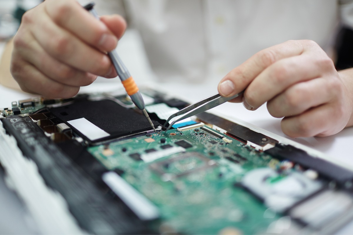
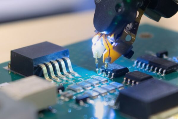
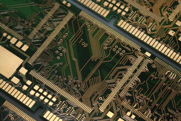
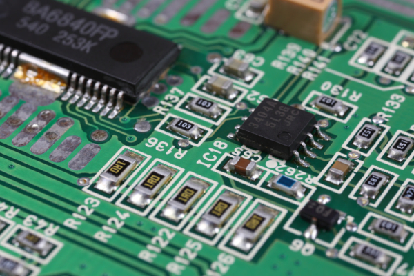
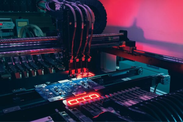
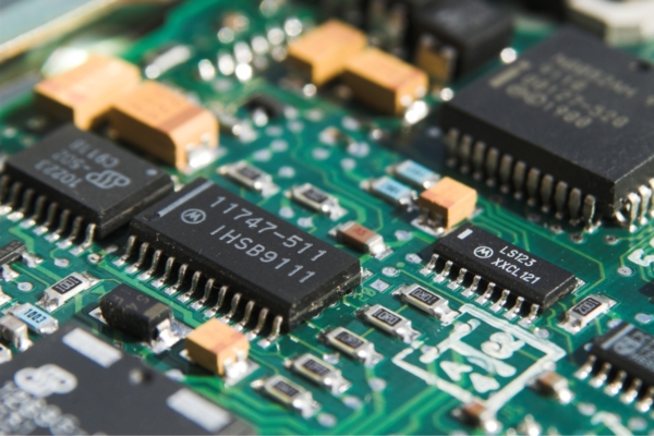
The rapid advancement of technology relies heavily on the ability to quickly iterate and refine electronic systems. In this dynamic environment, prototype circuit board assembly (PCBA) is not just a preliminary step but a crucial stage where innovation is tested and refined. It is during this phase that theoretical designs are physically realized, revealing unforeseen challenges and opportunities for optimization. Prototyping is more than just creating a functional model; it is a comprehensive process of understanding, refinement, and validation that bridges the gap between a concept and a market-ready product. For example, the development of early medical imaging devices involved initial prototypes with noise and artifacts. Through iterative improvements, these prototypes evolved into the high-resolution, life-saving diagnostic tools we use today, highlighting the transformative power of prototyping.
Design for Manufacturability (DFM) and Design for Assembly (DFA) in the Prototyping Phase
The success of a prototype is largely determined during the design phase. Design for Manufacturability (DFM) and Design for Assembly (DFA) are fundamental principles that dictate the ease, efficiency, and success of the assembly process.
Component Selection and Placement Optimization
Component selection goes beyond functional specifications. Factors like package size, lead configuration, availability in low volumes, and behavior under reflow temperatures must be carefully considered. A seemingly minor detail, such as choosing between a 0402 and a 0201 resistor, can significantly impact stencil design, placement accuracy, and solder joint reliability. For prototypes, sourcing specialized components with limited availability or long lead times adds complexity, requiring strategic partnerships with distributors and a deep understanding of the supply chain.
PCB Layout Considerations for Signal Integrity and Thermal Management
In high-speed digital and RF circuits, PCB layout is crucial for signal integrity. Trace routing, impedance matching, and layer stackup must be meticulously planned to minimize signal reflections, crosstalk, and electromagnetic interference (EMI). The increasing power densities of modern electronics also require sophisticated thermal management. Thermal vias, heat sinks, and careful component placement are essential to dissipate heat and prevent component failure. High-frequency designs, where minor layout imperfections can degrade performance, demand a deep understanding of electromagnetic principles and advanced simulation techniques.
Iterative Design Refinement: Bridging the Gap Between Simulation and Physical Realization
The prototyping phase provides crucial feedback for design refinement. While simulation tools offer valuable insights, they often cannot capture the full complexity of real-world behavior. Physical prototypes expose subtle interactions and unforeseen issues that simulations might miss. Data from prototype testing, such as signal integrity measurements, thermal profiles, or component failure analysis, provides invaluable feedback for iterative design improvements. This iterative process, where each prototype informs the next, is essential for bridging the gap between theoretical models and physical realization.
Core Assembly Processes for Prototype PCBs
Transforming a bare board into a functional assembly involves a carefully orchestrated sequence of processes, each requiring precision and control.
Solder Paste Application: Stencil Design, Paste Rheology, and Deposition Techniques
Solder paste application is a critical step where defects can easily occur. The choice of solder paste, including its alloy composition, flux type, and particle size distribution, directly impacts solder joint quality. Stencil design, particularly aperture size and shape, must be tailored to the components and PCB layout. The paste’s rheology, or flow characteristics under pressure, dictates deposition precision. Advanced techniques like step stencils and nano-coated stencils are used to address challenges in printing fine-pitch components and ensuring consistent paste release. The interplay of these factors determines the success of subsequent assembly steps.
Component Placement: Precision, Automation, and Handling of Sensitive Devices
Modern pick-and-place machines can place thousands of components per hour with remarkable accuracy. However, the prototype environment often presents unique challenges. Handling moisture-sensitive devices (MSDs) requires meticulous control of humidity and exposure time to prevent damage during reflow. Placing small, delicate components like 01005 passives or fine-pitch BGAs demands exceptional accuracy and gentle handling. Prototype runs often involve frequent setup changes, requiring flexible machines and efficient programming to minimize downtime.
Reflow Soldering: Profile Optimization, Atmosphere Control, and Defect Mitigation
Reflow soldering, the process of creating solder joints by melting solder paste, involves a delicate balance of temperature and time. The reflow profile, a sequence of temperature ramps and dwells, must be optimized for the specific board and component mix. Inert atmospheres, typically nitrogen, are used to minimize oxidation and improve solder wetting. However, defects like tombstoning, solder beading, and voiding can still occur. These defects, often subtle and difficult to detect, can significantly impact long-term reliability.
Wave Soldering: Applicability, Process Parameters, and Considerations for Mixed-Technology Boards
While reflow soldering dominates surface-mount technology (SMT) assembly, wave soldering remains relevant for through-hole components and some mixed-technology boards. This process involves passing the board over a wave of molten solder, creating joints on the underside. Controlling wave height, conveyor speed, flux application, and preheat temperature is crucial for good solder penetration and minimizing defects like bridging and icicling. However, the increasing use of SMT components and the challenges of soldering mixed-technology boards have led to a decline in wave soldering for prototypes.
Selective Soldering: Addressing Complex Geometries and Minimizing Thermal Stress
Selective soldering is valuable when specific components or areas of a board require soldering while minimizing thermal stress on adjacent components. This process uses programmable nozzles to apply solder and heat only to designated areas. Selective soldering is useful for assembling boards with complex geometries, heat-sensitive components, or components close to previously soldered parts. The ability to precisely control the soldering process makes it an indispensable tool for prototype assembly.
Advanced Assembly Techniques for High-Density and Specialized Prototypes
The drive towards miniaturization and increased functionality has led to advanced packaging technologies, each presenting unique assembly challenges.
Micro-BGA and Chip-Scale Package (CSP) Assembly
Micro-BGAs and CSPs, with their fine-pitch interconnects and small size, push the boundaries of assembly technology. These packages require ultra-precise alignment during placement, often using vision systems with sub-micron accuracy. Underfill, a capillary-action adhesive, is frequently used to enhance mechanical robustness and mitigate thermal cycling effects. Reflow profile optimization is critical to ensure proper solder joint formation without damaging the package. The small solder balls used in these packages are susceptible to voiding, necessitating meticulous process control and often requiring X-ray inspection to verify joint integrity.
Package-on-Package (PoP) and System-in-Package (SiP) Integration
PoP and SiP technologies enable the integration of multiple dies within a single package. PoP involves stacking packages vertically, while SiP integrates multiple dies and passive components into a single substrate. These techniques offer advantages in miniaturization, performance, and reduced interconnect lengths. However, they also introduce complexity to the assembly process. Stacking packages requires precise alignment and specialized bonding techniques. SiP assembly often involves intricate wire bonding or flip-chip processes to interconnect components. Thermal management is a paramount concern due to high component density and the close proximity of heat-generating dies.
Assembly of Flexible and Rigid-Flex PCBs
Flexible and rigid-flex PCBs combine flexible and rigid substrates, offering advantages in applications requiring flexibility or dynamic flexing. Assembling these boards presents unique challenges. Handling flexible substrates requires specialized fixtures and tooling to prevent damage or distortion. Component placement on flexible circuits must account for potential substrate movement during handling and reflow. Soldering techniques may need to be adapted for the lower thermal conductivity of flexible materials. The transition zones between rigid and flexible sections are susceptible to stress and require careful design and assembly for long-term reliability.
Embedded Component Technologies
Embedded component technology integrates passive and active components within the PCB layers, offering miniaturization and improved performance. Embedding components reduces interconnect lengths, improves signal integrity, and enhances reliability. However, it introduces manufacturing complexities. Fabricating embedded component boards requires specialized materials and processes, such as sequential lamination and laser via drilling. The assembly process must be carefully controlled to avoid damaging embedded components during subsequent steps. Testing and rework of embedded components pose unique challenges, often requiring specialized techniques and equipment.
Inspection and Testing of Prototype Assemblies
Thorough inspection and testing are essential to ensure the quality, functionality, and reliability of prototype assemblies.
Automated Optical Inspection (AOI): Defect Detection and Process Control
AOI systems use high-resolution cameras and image processing algorithms to detect assembly defects, including missing or misplaced components, incorrect orientation, solder bridges, and insufficient solder. AOI provides rapid and comprehensive inspection, making it invaluable for process control and quality assurance. However, its effectiveness relies on proper programming and optimization for each board design. The system must be trained to recognize acceptable variations and distinguish them from true defects. Lighting conditions, component variations, and board surface finish can impact AOI performance, necessitating careful calibration and monitoring.
X-ray Inspection: Unveiling Hidden Solder Joints and Internal Defects
X-ray inspection provides a non-destructive way to visualize solder joints beneath components like BGAs and QFNs, where optical inspection is impossible. X-ray imaging can reveal hidden defects like voids, cracks, and insufficient solder, which can impact long-term reliability. Different types of X-ray systems, including 2D and 3D (laminography or tomography), offer varying levels of detail. 2D X-ray is suitable for general inspection, while 3D X-ray provides detailed cross-sectional views for precise analysis of solder joint quality and internal component structure. The choice of X-ray system depends on the prototype’s requirements and the application’s criticality.
In-Circuit Testing (ICT) and Functional Testing: Validating Electrical Performance
ICT and functional testing verify the electrical performance of the assembled board. ICT uses a “bed of nails” fixture to contact test points, measuring component values and detecting shorts, opens, and other electrical defects. Functional testing involves powering up the board and verifying its functionality by simulating its operating environment. The choice between ICT and functional testing depends on test coverage requirements, cost, and board complexity. ICT offers comprehensive fault diagnosis but can be expensive for low-volume prototypes. Functional testing provides a realistic assessment of performance but may not offer detailed diagnostic information.
Reliability Testing: Assessing Long-Term Performance Under Stress
Reliability testing subjects the prototype to environmental stresses like temperature cycling, humidity exposure, vibration, and shock to evaluate long-term performance and identify potential failure mechanisms. Temperature cycling simulates thermal stresses during operation and can reveal weaknesses in solder joints or component attachments. Humidity testing assesses susceptibility to moisture ingress, which can lead to corrosion and electrical failures. Vibration and shock testing evaluate mechanical robustness and the ability to withstand physical stresses. Selecting appropriate reliability tests and parameters depends on the product’s intended application and expected environmental conditions.
Challenges and Considerations in Prototype PCB Assembly
Prototype PCBA presents unique challenges that distinguish it from high-volume production.
Managing Low-Volume, High-Mix Production Environments
Prototype assembly facilities must handle a constantly changing mix of board designs, component types, and assembly processes. This requires flexible manufacturing systems, efficient production planning, and meticulous tracking of materials and processes. Frequent setup changes, small lot sizes, and specialized tooling can impact production efficiency. Lean manufacturing principles, like setup reduction techniques and value stream mapping, are often used to streamline operations and minimize waste.
Sourcing and Handling of Specialized Components
Prototypes often use specialized components that may not be readily available in low volumes or may have long lead times. Sourcing these components requires relationships with specialized distributors, brokers, or manufacturers. Managing the inventory, ensuring proper storage conditions (especially for MSDs), and tracking usage across projects can be a logistical challenge.
Maintaining Process Control with Limited Production Runs
Establishing and maintaining process control in a low-volume environment, where only a few boards may be assembled for a given prototype, can be difficult. Statistical process control (SPC) techniques used in high-volume manufacturing may not be directly applicable due to limited sample sizes. Prototype assemblers often rely on meticulous documentation of process parameters, rigorous inspection and testing, and data analysis from previous builds to ensure consistent quality.
Addressing Rework and Modification Requirements
Prototypes are subject to design changes and modifications as testing reveals areas for improvement. Rework and modifications on densely populated boards can be challenging and carry the risk of damaging components or the board. Skilled technicians with expertise in rework techniques, such as component removal, site preparation, and re-soldering, are essential. Specialized rework equipment, including hot air stations, microscopes, and precision soldering tools, are necessary for complex modifications.
Emerging Trends and Future Directions in Prototype Assembly
The field of prototype PCBA is continuously evolving, driven by technological advancements and the increasing demands of electronic systems.
Additive Manufacturing and 3D Printing of PCBs
Additive manufacturing, or 3D printing, has the potential to revolutionize PCB fabrication. 3D printing technologies like inkjet printing and aerosol jet printing enable the creation of PCBs with complex geometries, embedded components, and customized interconnect structures. While still in early development for PCB manufacturing, 3D printing offers rapid prototyping, reduced lead times, and greater design flexibility. However, challenges remain in material properties, resolution, and scalability before 3D-printed PCBs can compete with conventional methods.
Automation and Robotics in Low-Volume Assembly
Collaborative robots (cobots), designed to work alongside human operators, are opening new possibilities for automation in low-volume assembly. Cobots can be programmed to perform repetitive tasks like component placement, dispensing, and inspection, freeing up human technicians for more complex tasks. Vision systems and artificial intelligence enhance robot capabilities, enabling them to adapt to variations and perform more sophisticated operations.
Artificial Intelligence and Machine Learning for Process Optimization
Artificial intelligence (AI) and machine learning (ML) are finding applications in PCB assembly, particularly in process optimization and defect prediction. By analyzing large datasets of process parameters, inspection results, and test data, AI and ML algorithms can identify patterns and correlations that may not be apparent to humans. This information can optimize process parameters, predict potential defects, and improve assembly yields. However, successful implementation requires access to large, well-structured datasets and expertise in data analysis and algorithm development.
Sustainable Manufacturing Practices in PCB Assembly
Environmental concerns are driving sustainable manufacturing practices in the electronics industry, including PCB assembly. Efforts are underway to reduce waste, conserve energy, and minimize hazardous materials. Lead-free soldering has become the industry standard, eliminating lead, a toxic heavy metal. Recycling programs for electronic waste are gaining traction, reducing the environmental impact of discarded PCBs. The development of bio-based and biodegradable materials for PCB substrates and components is another area of research, aiming to further reduce the environmental footprint of electronic products.
The Evolving Landscape of Prototype Circuit Board Assembly
Prototype circuit board assembly is a critical link between design and realization, a testing ground where innovation is refined and validated. The intricacies of this field, from DFM and DFA to advanced packaging and low-volume production challenges, demand technical expertise, process control, and adaptability. As we move towards miniaturization, increased functionality, and rapid technological change, the landscape of prototype assembly will continue to evolve. Emerging trends like additive manufacturing, robotics, AI, and sustainable practices promise to reshape the field, offering new tools and capabilities. Mastering these intricacies will remain paramount for transitioning innovative designs into market-ready products and driving the advancement of electronic systems that underpin our interconnected world. The journey from concept to prototype to product is challenging, but it is within this crucible that the future of technology is forged.
