PCB assembly, also known as PCBA, is the process of populating a printed circuit board with electronic components and creating the necessary electrical connections to form a functional circuit. It involves a series of precise steps that combine human expertise with advanced automation to ensure the highest quality and reliability of the final product.
PCB assembly is distinct from PCB fabrication, which focuses on the creation of the bare circuit board itself. Fabrication involves the lamination of conductive copper layers, the application of solder mask and silkscreen, and the drilling of holes for component placement. Once the bare PCB is fabricated, it moves on to the assembly stage, where the real magic happens.
The main steps involved in PCB assembly include solder paste application, component placement, soldering, inspection, and testing. Each step requires meticulous attention to detail and adherence to industry standards to ensure the integrity and functionality of the assembled board.
The importance of PCB assembly cannot be overstated. It is the process that brings life to the intricate designs created by electrical engineers, transforming a static circuit board into a dynamic, functioning device. The quality of the assembly directly impacts the performance, reliability, and longevity of the final product, making it a critical aspect of electronics manufacturing.
Key Components of a PCB
Before diving into the assembly process, let’s take a moment to understand the key components that make up a PCB:
- Substrate: The substrate is the foundation of the PCB, providing the rigid base material on which the other layers are built. It is typically made of FR-4, a glass-reinforced epoxy laminate, which offers excellent electrical insulation and mechanical stability.
- Copper Layers: PCBs feature one or more layers of copper foil laminated onto the substrate. These copper layers form the conductive pathways that carry electrical signals between components. The number of copper layers determines the complexity and density of the circuit.
- Solder Mask: A layer of polymer coating, known as solder mask, is applied over the copper layers to protect them from oxidation and prevent accidental short circuits during soldering. The solder mask also provides electrical insulation between adjacent traces and pads.
- Silkscreen: The silkscreen layer is a printed overlay that adds text, logos, and component identifiers to the PCB surface. It helps in the assembly process by providing visual cues for component placement and aids in troubleshooting and maintenance.
With a basic understanding of the key components, let’s now explore the various aspects of PCB assembly in greater detail.
PCB Design and Layers
PCB design is a critical aspect of the assembly process, as it lays the foundation for the functionality and manufacturability of the final product. A well-designed PCB not only ensures the proper placement and interconnection of components but also takes into account factors such as signal integrity, thermal management, and manufacturing constraints.
The number and arrangement of layers in a PCB play a significant role in determining its complexity and functionality. Single-layer PCBs, with conductive traces on only one side of the substrate, are the simplest and most cost-effective option for basic circuits. Double-layer PCBs, with traces on both sides, offer increased routing flexibility and higher component density. Multi-layer PCBs, consisting of three or more conductive layers separated by insulating material, are used for more complex designs requiring advanced signal routing and power distribution.
The choice of substrate material is another important consideration in PCB design. While FR-4 is the most common substrate, other materials such as polyimide and metal core PCBs offer specific advantages for certain applications. Flexible PCBs, made from thin, bendable materials, are ideal for wearable electronics and space-constrained designs. Metal core PCBs, with a metal substrate for improved heat dissipation, are used in high-power applications.
The PCB design process typically begins with schematic capture, where the logical connections between components are defined using specialized software. The schematic is then translated into a physical layout, taking into account factors such as component footprints, trace widths, and spacing requirements. Design for Manufacturability (DFM) guidelines are followed to ensure that the PCB can be efficiently and reliably manufactured.
Once the PCB design is finalized, it undergoes a series of checks and simulations to verify its functionality and adherence to industry standards. This includes signal integrity analysis, thermal simulations, and design rule checks (DRC) to identify any potential issues before manufacturing begins.
The importance of a well-designed PCB cannot be overstated. It directly impacts the assembly process, determining the ease of component placement, the reliability of solder joints, and the overall quality of the final product. A poorly designed PCB can lead to manufacturing challenges, increased defects, and compromised performance.
Types of PCB Assembly Technologies
PCB assembly technologies have evolved over the years to meet the increasing demands for miniaturization, high component density, and faster production cycles. The two main types of PCB assembly technologies are Surface Mount Technology (SMT) and Through-Hole Technology (THT).
Surface Mount Technology (SMT)
Surface Mount Technology (SMT) is the dominant assembly method in modern electronics manufacturing. It involves the placement of components directly onto the surface of the PCB, without the need for drilled holes. SMT components, such as resistors, capacitors, and integrated circuits, have small metal leads or pads that are soldered to corresponding pads on the PCB surface.
The SMT assembly process begins with the application of solder paste onto the PCB pads using a stencil printing method. The solder paste, a mixture of tiny solder particles suspended in flux, is precisely deposited onto the pads. Next, a pick-and-place machine automatically picks up the SMT components from reels or trays and places them onto the solder paste-coated pads with high precision.
Once all the components are placed, the PCB undergoes a reflow soldering process. The board is passed through a reflow oven, where it is subjected to a carefully controlled temperature profile. The solder paste melts, forming a strong mechanical and electrical bond between the component leads and the PCB pads. The board is then cooled, allowing the solder joints to solidify.
SMT offers several advantages over THT, including:
- Miniaturization: SMT components are smaller and have a lower profile compared to THT components, enabling higher component density and more compact designs.
- Faster Assembly: The automated nature of SMT assembly allows for faster placement rates and shorter production cycles.
- Improved Reliability: SMT components have shorter lead lengths and are less susceptible to mechanical stress, resulting in improved reliability and reduced defects.
Common SMT component packages include 0402, 0603, SOIC, QFP, and BGA. These packages offer different sizes, lead configurations, and mounting options to suit various design requirements.
Through-Hole Technology (THT)
Through-Hole Technology (THT) is an older but still relevant assembly method, particularly for components that require stronger mechanical bonds or higher power handling capabilities. THT components have long leads that are inserted through drilled holes in the PCB and soldered on the opposite side.
The THT assembly process involves the manual or automated insertion of component leads into the corresponding holes on the PCB. The board is then flipped over, and the protruding leads are soldered, typically using a wave soldering machine. The wave soldering process involves passing the board over a molten solder wave, which coats the component leads and creates a strong mechanical and electrical connection.
THT offers certain advantages, such as:
- Stronger Mechanical Bonds: The leads of THT components extend through the PCB, providing a more robust mechanical connection compared to SMT.
- Better Power Handling: THT components, such as large capacitors and transformers, can handle higher power levels due to their larger size and stronger connections.
Common THT component types include DIP (Dual Inline Package), axial and radial leaded components, and connectors.
Mixed Technology Assembly
In some cases, PCBs may require a combination of both SMT and THT components. This is known as mixed technology assembly. Mixed assembly is used when certain components are not available in SMT packages or when specific design requirements necessitate the use of THT components.
Mixed technology assembly presents challenges in terms of process sequencing and compatibility. Typically, SMT components are assembled first, followed by the insertion and soldering of THT components. Care must be taken to ensure that the THT soldering process does not damage or dislodge the previously assembled SMT components.
The choice between SMT and THT assembly depends on various factors, including component availability, design requirements, production volume, and cost considerations. SMT is generally preferred for high-volume production and designs requiring miniaturization, while THT is used for specific components or in applications demanding stronger mechanical bonds.
PCB Assembly Process Steps
The PCB assembly process involves a series of precise steps that transform a bare circuit board into a fully functional electronic assembly. Each step plays a critical role in ensuring the quality, reliability, and functionality of the final product.
Solder Paste Application
The first step in the PCB assembly process is the application of solder paste onto the PCB pads. Solder paste is a mixture of tiny solder particles suspended in flux, which helps to clean and protect the metal surfaces during soldering. The solder paste is applied using a stencil printing method, which ensures precise and consistent deposition of the paste onto the pads.
The stencil is a thin metal sheet with apertures that correspond to the PCB pad locations. It is aligned with the PCB, and the solder paste is spread across the stencil surface using a squeegee blade. The paste is forced through the apertures, depositing a controlled amount onto the pads. The stencil is then removed, leaving the solder paste in the desired locations.
Proper solder paste application is crucial for achieving reliable solder joints. The amount of paste deposited, the consistency of the paste, and the accuracy of the stencil alignment all contribute to the quality of the final solder connections.
Component Placement
Once the solder paste is applied, the next step is the placement of components onto the PCB. In modern PCB assembly, this process is typically automated using pick-and-place machines. These machines are equipped with high-precision robotic arms and vision systems that accurately pick up components from reels or trays and place them onto the solder paste-coated pads.
The pick-and-place machine is programmed with the component placement data, which includes the location, orientation, and type of each component. It uses this information to rapidly and accurately place the components onto the PCB. The machine can handle a wide range of component sizes and types, from tiny surface-mount devices to larger through-hole components.
For high-volume production, automated pick-and-place machines offer significant advantages in terms of speed, accuracy, and consistency. They can place thousands of components per hour with exceptional precision, reducing the risk of human error and improving overall assembly efficiency.
In some cases, such as low-volume production or prototyping, manual component placement may be used. Skilled technicians carefully place the components onto the PCB using tweezers or other hand tools. While manual placement is slower and more labor-intensive, it offers flexibility for custom or complex designs.
Reflow Soldering
After the components are placed, the PCB undergoes a reflow soldering process to permanently attach the components to the board. Reflow soldering involves exposing the PCB to a carefully controlled temperature profile that melts the solder paste, forming a strong mechanical and electrical bond between the component leads and the PCB pads.
The PCB is passed through a reflow oven, which consists of several heating zones with precise temperature control. The temperature profile is designed to gradually heat the PCB, activating the flux in the solder paste and allowing it to clean the metal surfaces. As the temperature rises, the solder particles melt and flow, forming a liquid solder joint around the component leads and pads.
The peak temperature in the reflow process is carefully controlled to ensure that the solder melts completely without damaging the components or the PCB substrate. The duration of the peak temperature is also critical, as it allows sufficient time for the solder to wet the surfaces and form a reliable joint.
After the peak temperature is reached, the PCB is gradually cooled, allowing the molten solder to solidify and create a permanent connection between the components and the PCB. Proper cooling is essential to prevent thermal stress and ensure the formation of strong, reliable solder joints.
Inspection and Quality Control
Once the reflow soldering process is complete, the assembled PCB undergoes a series of inspections and quality control checks to ensure that it meets the required standards and specifications. Inspection is a critical step in identifying any defects or issues that may affect the functionality or reliability of the final product.
Visual inspection is the most basic form of quality control, where trained operators manually examine the PCB for visible defects such as missing components, solder bridges, or poor solder joints. Visual inspection relies on the skill and experience of the operator to identify potential issues.
Automated Optical Inspection (AOI) is a more advanced inspection method that uses high-resolution cameras and image processing software to detect defects on the PCB surface. AOI systems can quickly and accurately identify a wide range of defects, including missing components, incorrect component placement, solder bridges, and insufficient solder coverage. AOI offers significant advantages in terms of speed, consistency, and repeatability compared to manual inspection.
X-ray inspection is another important quality control technique, particularly for PCBs with hidden or obscured solder joints, such as those found in Ball Grid Array (BGA) packages or multi-layer boards. X-ray systems use high-energy radiation to create detailed images of the internal structure of the PCB, allowing operators to identify defects such as voids, cracks, or misaligned components that may not be visible from the surface.
In addition to visual and automated inspection, functional testing is performed to verify that the assembled PCB operates as intended. This may involve applying power to the board and measuring various electrical parameters, such as voltage, current, and signal integrity. Functional testing ensures that the PCB meets the design specifications and performs reliably under normal operating conditions.
Quality control metrics, such as defects per million opportunities (DPMO) or first-pass yield (FPY), are used to track and monitor the performance of the assembly process. These metrics provide valuable insights into the efficiency and effectiveness of the assembly line, allowing manufacturers to identify areas for improvement and implement corrective actions to reduce defects and improve overall quality.
Through-Hole Component Insertion
While surface-mount technology (SMT) has become the dominant assembly method for modern PCBs, some designs still require the use of through-hole components. These components have long leads that are inserted through drilled holes in the PCB and soldered on the opposite side.
The through-hole component insertion process can be performed manually or using automated insertion machines. In manual insertion, skilled operators carefully insert the component leads into the corresponding holes on the PCB, ensuring proper alignment and orientation. This method is typically used for low-volume production or for components that are not suitable for automated insertion.
Automated insertion machines, on the other hand, use robotic arms and feeders to rapidly and accurately insert through-hole components into the PCB. These machines can handle a wide range of component types and sizes, and they offer significant advantages in terms of speed and consistency compared to manual insertion.
Once the through-hole components are inserted, the PCB undergoes a wave soldering process to create a permanent electrical and mechanical connection between the component leads and the PCB. Wave soldering involves passing the PCB over a molten solder wave, which coats the component leads and fills the holes, forming a strong solder joint.
Final Inspection and Testing
After all the components are assembled and soldered, the PCB undergoes a final inspection and testing process to ensure that it meets the required quality standards and functions as intended. This step is critical for catching any remaining defects or issues before the product is shipped to the customer.
The final inspection may involve a combination of visual inspection, automated optical inspection (AOI), and X-ray inspection to verify the integrity of the solder joints, the correct placement of components, and the overall quality of the assembly.
In addition to visual inspection, functional testing is performed to validate the electrical performance of the PCB. This may involve applying power to the board and measuring various parameters, such as voltage, current, and signal integrity, to ensure that the PCB operates within the specified tolerances.
Depending on the complexity and criticality of the application, additional testing may be performed, such as environmental testing (e.g., temperature, humidity, vibration) or accelerated life testing to assess the long-term reliability of the PCB under various operating conditions.
Thorough final inspection and testing are essential for ensuring that the assembled PCB meets the highest quality standards and performs reliably in the field. Any defects or issues identified during this stage are carefully documented and addressed through rework or repair processes to maintain the integrity of the final product.
Automated vs. Manual Assembly
In the world of PCB assembly, manufacturers have the option to choose between automated and manual assembly methods. Each approach has its own advantages and considerations, and the choice often depends on factors such as production volume, component complexity, and cost constraints.
Automated Assembly
Automated PCB assembly relies on advanced equipment and robotics to perform the various steps of the assembly process, from solder paste application and component placement to soldering and inspection. Automated assembly offers several key advantages:
- Speed: Automated assembly lines can operate at much higher speeds compared to manual assembly, with pick-and-place machines capable of placing thousands of components per hour. This increased speed translates to shorter production cycles and faster time-to-market for electronic products.
- Precision: Automated equipment, such as pick-and-place machines and reflow ovens, is designed to operate with extremely high precision and repeatability. This ensures consistent placement of components, accurate solder joint formation, and minimal defects, resulting in higher overall quality of the assembled PCBs.
- Consistency: Automated assembly processes are highly repeatable and consistent, as the equipment follows predefined programs and parameters. This consistency is particularly important for high-volume production, where maintaining uniform quality across large batches of PCBs is critical.
Automated assembly is most beneficial for high-volume production runs, where the speed, precision, and consistency of the equipment can significantly reduce costs and improve efficiency. The initial investment in automated equipment may be higher compared to manual assembly, but the long-term benefits in terms of productivity and quality often justify the investment.
Manual Assembly
Manual PCB assembly involves skilled technicians performing the various assembly tasks by hand, using tools such as soldering irons, tweezers, and magnifying lenses. While manual assembly may seem less efficient compared to automated methods, it still has its place in the electronics manufacturing industry.
- Flexibility: Manual assembly offers greater flexibility in terms of accommodating design changes, prototyping, and low-volume production. Skilled technicians can quickly adapt to modifications in component placement or soldering requirements without the need for extensive programming or equipment setup.
- Lower Initial Costs: Setting up a manual assembly line typically requires lower upfront investment compared to automated equipment. This makes manual assembly an attractive option for small-scale operations, startups, or businesses with limited capital.
- Prototyping and Complex Assemblies: Manual assembly is often preferred for prototyping and low-volume production, where the cost and time required to program automated equipment may not be justified. Additionally, manual assembly can handle complex or non-standard components that may be difficult to place using automated machines.
Manual assembly relies heavily on the skills and experience of the technicians involved. Proper training, attention to detail, and adherence to industry standards are essential for ensuring the quality and reliability of manually assembled PCBs.
Comparison Table
Here’s a comparison table summarizing the key differences between automated and manual PCB assembly:
| Factor | Automated Assembly | Manual Assembly |
|---|---|---|
| Speed | High | Low |
| Precision | High | Depends on operator skill |
| Consistency | High | Varies |
| Flexibility | Limited | High |
| Initial Costs | High | Low |
| Suitable for | High-volume production | Low-volume, prototypes, complex assemblies |
The choice between automated and manual assembly depends on various factors, including production volume, product complexity, available resources, and target market. Many electronics manufacturers employ a combination of both methods, leveraging the strengths of each approach to optimize their assembly processes and meet specific production requirements.
Quality Assurance in PCB Assembly
Quality assurance is a critical aspect of PCB assembly, as it directly impacts the reliability, performance, and longevity of the final product. Implementing robust quality assurance processes throughout the assembly cycle helps to identify and prevent defects, ensure conformance to specifications, and maintain high standards of workmanship.
Visual Inspection
Visual inspection is the most basic form of quality control in PCB assembly. It involves trained operators manually examining the assembled PCBs for visible defects and anomalies. Visual inspection typically covers aspects such as component placement, solder joint quality, and general board cleanliness.
During visual inspection, operators look for issues such as missing or misaligned components, solder bridges, insufficient or excessive solder, and any signs of physical damage to the PCB or components. Visual inspection relies heavily on the skill, experience, and attention to detail of the operators involved.
While visual inspection is an important first line of defense against defects, it has limitations in terms of speed, consistency, and the ability to detect hidden or subtle issues. As a result, visual inspection is often complemented by more advanced inspection methods to ensure comprehensive quality control.
Automated Optical Inspection (AOI)
Automated Optical Inspection (AOI) is a powerful tool for detecting surface-level defects on assembled PCBs. AOI systems use high-resolution cameras and advanced image processing algorithms to capture and analyze images of the PCB surface, comparing them against predefined templates or design data.
AOI systems can quickly and accurately identify a wide range of defects, including:
- Missing or misaligned components
- Incorrect component polarity or orientation
- Solder bridges or short circuits
- Insufficient or excessive solder
- Lifted or tombstoned components
- Damaged or missing solder mask
The advantages of AOI include its speed, consistency, and ability to detect defects that may be difficult to spot with the naked eye. AOI systems can inspect hundreds of PCBs per hour, providing rapid feedback on the quality of the assembly process. Additionally, AOI data can be used for process optimization and traceability purposes.
AOI has limitations in terms of detecting defects that are hidden from view, such as issues with solder joint integrity beneath components or within multi-layer PCBs. In such cases, additional inspection methods may be necessary.
X-ray Inspection
X-ray inspection is a powerful technique for detecting defects that are not visible from the surface of the PCB. It is particularly useful for inspecting solder joints in Ball Grid Array (BGA) packages, multi-layer boards, or other components with hidden connections.
X-ray inspection systems use high-energy X-rays to penetrate the PCB and create detailed images of the internal structure. These images can reveal defects such as:
- Voids or cracks in solder joints
- Misaligned or bridged balls in BGA packages
- Insufficient or excessive solder in through-hole joints
- Broken or damaged traces within the PCB layers
X-ray inspection provides valuable insights into the integrity of the solder joints and the overall quality of the assembly. It allows manufacturers to identify and address issues that may not be detectable through other inspection methods, ensuring the reliability and performance of the final product.
In-Circuit Testing (ICT)
In-Circuit Testing (ICT) is a powerful technique for verifying the electrical functionality of assembled PCBs. ICT involves using specialized test fixtures and equipment to apply electrical signals to specific points on the PCB and measure the response.
During ICT, the assembled PCB is placed in a test fixture that makes contact with the board through a bed of nails or probes. The test equipment then applies a series of electrical tests to verify the presence, orientation, and value of components, as well as the integrity of the interconnections between them.
ICT can detect a wide range of electrical faults, including:
- Open or short circuits
- Incorrect component values or tolerances
- Reversed or missing components
- Defective or damaged components
The advantages of ICT include its ability to quickly and accurately identify electrical issues that may not be detectable through visual or optical inspection methods. ICT can test a large number of points on the PCB in a matter of seconds, providing rapid feedback on the electrical functionality of the assembly.
ICT requires the development of specialized test fixtures and programs, which can be time-consuming and costly. Additionally, ICT may not be suitable for certain types of components or board designs that are difficult to access or probe.
Functional Testing
Functional testing is a critical step in ensuring that the assembled PCB performs as intended in its final application. It involves subjecting the PCB to a series of operational tests that simulate real-world conditions and verify its functionality, performance, and reliability.
Functional testing typically covers aspects such as:
- Power-on and boot-up sequences
- Input/output functionality
- Communication protocols and interfaces
- Signal integrity and timing
- Environmental stress testing (e.g., temperature, humidity, vibration)
During functional testing, the PCB is connected to test equipment that provides the necessary inputs and monitors the outputs. The test scenarios are designed to exercise the various functions and features of the PCB, ensuring that it meets the specified requirements and operates reliably under different conditions.
Functional testing is crucial for identifying issues that may not be detectable through other inspection or testing methods. It helps to validate the overall design, firmware, and software integration, as well as uncover any compatibility or interoperability issues.
Thorough functional testing is essential for ensuring the quality and reliability of the final product, particularly in mission-critical or safety-related applications.
Quality Control Metrics
To effectively monitor and improve the quality of the PCB assembly process, manufacturers often rely on a set of quality control metrics. These metrics provide quantitative measures of the assembly process performance and help identify areas for improvement.
Some common quality control metrics used in PCB assembly include:
- Defects per Million Opportunities (DPMO): DPMO measures the number of defects found per million opportunities for defects. It provides a standardized way to compare the quality of different assembly processes or suppliers.
- First Pass Yield (FPY): FPY represents the percentage of PCBs that pass all quality inspections and tests on the first attempt, without requiring rework or repair. A high FPY indicates an efficient and well-controlled assembly process.
- Rework Rate: The rework rate measures the percentage of PCBs that require additional work or repairs after the initial assembly. A low rework rate is desirable, as it indicates a high level of quality and efficiency in the assembly process.
- Scrap Rate: The scrap rate represents the percentage of PCBs that are deemed unusable and must be discarded due to defects or quality issues. Minimizing the scrap rate helps to reduce waste and improve overall productivity.
By regularly monitoring and analyzing these quality control metrics, manufacturers can identify trends, pinpoint areas for improvement, and implement corrective actions to enhance the overall quality and efficiency of the PCB assembly process.
Continuous improvement initiatives, such as Six Sigma or Lean Manufacturing, can be applied to the PCB assembly process to systematically reduce defects, minimize waste, and optimize resource utilization. By embracing a data-driven approach to quality assurance and fostering a culture of continuous improvement, PCB assembly manufacturers can consistently deliver high-quality products that meet or exceed customer expectations.
PCB Assembly Equipment
To achieve the high levels of precision, consistency, and efficiency required in modern PCB assembly, manufacturers rely on a range of specialized equipment. This equipment plays a critical role in automating various stages of the assembly process, from solder paste application and component placement to soldering and inspection.
Solder Paste Printer
Solder paste printers are used to apply solder paste onto the PCB pads prior to component placement. These machines use a stencil printing method to deposit a precise amount of solder paste onto the pads, ensuring a consistent and reliable solder joint formation.
The solder paste printer typically consists of a stencil frame, a squeegee blade, and a vision system for alignment. The stencil is a thin metal sheet with apertures that correspond to the PCB pad locations. The squeegee blade moves across the stencil, forcing the solder paste through the apertures and onto the pads.
Precise control over the solder paste volume, consistency, and placement is critical for achieving high-quality solder joints. Modern solder paste printers often incorporate features such as automatic stencil cleaning, vision-based alignment, and closed-loop process control to ensure optimal paste deposition.
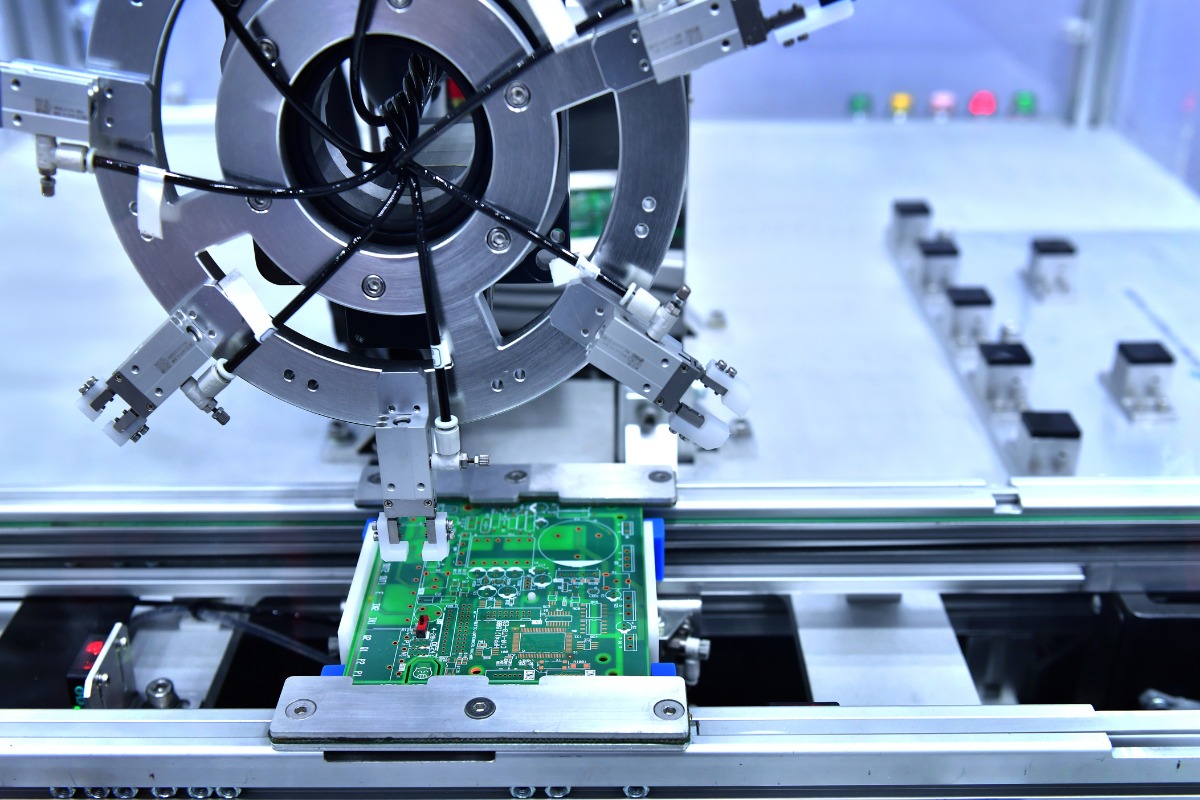
Pick and Place Machines
Pick and place machines are the workhorses of the PCB assembly line, responsible for rapidly and accurately placing components onto the PCB. These machines use robotic arms equipped with vacuum nozzles or grippers to pick up components from reels or trays and place them onto the solder paste-coated pads.
Modern pick and place machines are highly sophisticated, capable of placing thousands of components per hour with exceptional accuracy. They incorporate advanced vision systems and software algorithms to ensure precise component alignment and orientation.
The speed and accuracy of pick and place machines are critical factors in determining the overall throughput and quality of the assembly process. High-speed machines can place components at rates exceeding 100,000 parts per hour, while maintaining placement accuracies in the range of ±50 microns or better.
Pick and place machines come in various configurations, from compact desktop models for low-volume production to large, multi-head systems for high-volume manufacturing. They can handle a wide range of component types and sizes, from tiny chip resistors to large integrated circuits and connectors.
Reflow Ovens
Reflow ovens are used to permanently bond the components to the PCB by melting the solder paste and forming a strong mechanical and electrical connection. These ovens expose the PCB to a carefully controlled temperature profile that activates the flux, melts the solder, and allows it to wet the component leads and pads.
Reflow ovens typically consist of multiple heating zones, each with independent temperature control. The PCB passes through these zones on a conveyor belt, following a specific temperature profile that is optimized for the solder paste and components used.
The temperature profile in a reflow oven is critical for achieving reliable solder joints. It must provide sufficient heat to fully melt the solder and activate the flux, while avoiding thermal damage to the components or PCB substrate. The peak temperature, duration, and cooling rate are carefully controlled to ensure optimal solder joint formation.
Modern reflow ovens often incorporate features such as nitrogen atmosphere control, which helps to reduce oxidation and improve solder joint quality. They may also include advanced process monitoring and control systems to ensure consistent and repeatable results.
Wave Soldering Machines
Wave soldering machines are used for soldering through-hole components to the PCB. These machines consist of a molten solder reservoir and a pump that generates a standing wave of solder. The PCB is passed over the solder wave, allowing the component leads to be coated and bonded to the PCB.
Wave soldering is typically used for PCBs with a mix of surface-mount and through-hole components. The surface-mount components are first placed and reflowed, followed by the insertion of through-hole components. The PCB is then passed over the solder wave to complete the soldering process.
Wave soldering machines require careful control over parameters such as solder temperature, wave height, and conveyor speed to ensure consistent and reliable solder joints. They may also incorporate features such as preheating zones, fluxing systems, and cooling stations to optimize the soldering process.
Inspection Equipment
Inspection equipment plays a vital role in ensuring the quality and reliability of the assembled PCBs. Various types of inspection equipment are used throughout the assembly process to detect defects, verify component placement, and assess solder joint quality.
- Automated Optical Inspection (AOI): AOI systems use high-resolution cameras and advanced image processing algorithms to inspect the PCB surface for defects such as missing components, solder bridges, or incorrect component orientation. They can quickly scan the entire PCB and identify potential issues, reducing the need for manual inspection.
- X-ray Inspection: X-ray inspection systems are used to examine solder joints and internal structures that are not visible from the surface of the PCB. They are particularly useful for inspecting Ball Grid Array (BGA) packages, multi-layer boards, or other components with hidden connections. X-ray inspection can reveal defects such as voids, cracks, or misaligned components.
- In-Circuit Testing (ICT): ICT equipment is used to verify the electrical functionality of the assembled PCB. It consists of a test fixture with probes that make contact with specific points on the PCB, allowing the equipment to apply electrical signals and measure the response. ICT can detect issues such as open or short circuits, incorrect component values, or missing components.
Inspection equipment helps to identify defects early in the assembly process, reducing the risk of costly rework or product failures in the field. By incorporating automated inspection systems and data analytics, manufacturers can monitor process performance, identify trends, and implement continuous improvement initiatives.
Cleaning Equipment
Cleaning equipment is used to remove flux residues, contaminants, and other debris from the assembled PCB. Proper cleaning is essential for ensuring the long-term reliability and performance of the PCB, particularly in applications where cleanliness is critical, such as medical devices or aerospace systems.
Cleaning equipment can range from simple manual cleaning stations to fully automated inline cleaning systems. Common cleaning methods include:
- Aqueous Cleaning: Aqueous cleaning uses water-based solutions and detergents to remove flux residues and other contaminants from the PCB. The PCB is typically immersed in the cleaning solution, followed by rinsing and drying stages. Aqueous cleaning is effective for removing a wide range of contaminants and is environmentally friendly compared to solvent-based methods.
- Solvent Cleaning: Solvent cleaning uses organic solvents to dissolve and remove flux residues and other contaminants from the PCB. Common solvents include isopropyl alcohol, terpenes, and modified alcohols. Solvent cleaning is effective for removing stubborn contaminants and can be used for PCBs with sensitive components that may be damaged by aqueous cleaning.
- Plasma Cleaning: Plasma cleaning uses ionized gas to remove organic contaminants from the PCB surface. It is a dry, non-contact cleaning method that is particularly effective for removing fine particulates and residues from hard-to-reach areas. Plasma cleaning is often used for high-reliability applications or for PCBs with delicate components.


 Circuit Board Assembly")

 VS Printed Circuit Board Assemblies (PCBA)")