Krajobraz produkcji elektroniki przeszedł głęboką transformację w ostatnich dziesięcioleciach, w dużej mierze dzięki pojawieniu się i powszechnemu przyjęciu technologii montażu powierzchniowego (SMT). Aby naprawdę docenić znaczenie SMT, należy wziąć pod uwagę ograniczenia jej poprzedniczki, technologii przewlekanej. Technologia przewlekana, z wyprowadzeniami komponentów wkładanymi w wywiercone otwory i lutowanymi po przeciwnej stronie płytki, nakładała ograniczenia na gęstość komponentów i miniaturyzację. Pojawienie się SMT w latach 80. oznaczało zmianę paradygmatu, umożliwiając umieszczanie komponentów bezpośrednio na powierzchni płytek drukowanych (PCB). Ta pozornie prosta zmiana miała daleko idące konsekwencje, torując drogę dla mniejszych, lżejszych i bardziej zaawansowanych urządzeń elektronicznych.
Perspektywa historyczna: Od technologii przewlekanej do SMT
Podróż od technologii przewlekanej do SMT nie była rewolucją z dnia na dzień, ale raczej stopniową ewolucją napędzaną nieustannym dążeniem do miniaturyzacji i zwiększonej funkcjonalności. Wczesne procesy SMT napotykały wyzwania związane z dostępnością komponentów, dojrzałością sprzętu i niezawodnością procesu. Jednak nieodłączne zalety SMT, takie jak zmniejszony rozmiar płytki, lepsza wydajność elektryczna i przydatność do automatyzacji, szybko stały się oczywiste. Pionierzy w branżach takich jak elektronika użytkowa i telekomunikacja przyjęli SMT, napędzając innowacje w sprzęcie, materiałach i rozwoju procesów. Każde stopniowe ulepszenie bazowało na poprzednim, prowadząc do wyrafinowanego ekosystemu SMT, który mamy dzisiaj.
Fundamentalna zmiana: Miniaturyzacja i zwiększona funkcjonalność
Podstawową zaletą SMT jest jej zdolność do ułatwiania stosowania mniejszych komponentów i osiągania wyższej gęstości komponentów na PCB. Ta miniaturyzacja nie polega tylko na zmniejszaniu wymiarów fizycznych; chodzi o upakowanie większej funkcjonalności w danej przestrzeni. SMT umożliwia umieszczanie komponentów po obu stronach płytki, skutecznie podwajając dostępną powierzchnię. Ponadto krótsze wyprowadzenia i mniejsze rozmiary obudów komponentów SMT skutkują zmniejszoną indukcyjnością i pojemnością, co prowadzi do poprawy integralności sygnału i większych prędkości roboczych. Jest to szczególnie ważne w zastosowaniach wysokiej częstotliwości, gdzie integralność sygnału jest najważniejsza.
Wpływ SMT na różne branże: Krótki przegląd
Wpływ SMT jest wszechobecny, dotykając praktycznie każdej branży, która opiera się na elektronice. W elektronice użytkowej SMT umożliwiła rozwój smartfonów, tabletów, laptopów i niezliczonych innych urządzeń przenośnych. Przemysł motoryzacyjny wykorzystuje SMT do jednostek sterujących silnikiem, systemów informacyjno-rozrywkowych i zaawansowanych systemów wspomagania kierowcy (ADAS), gdzie niezawodność w trudnych warunkach jest krytyczna. W lotnictwie i kosmonautyce zdolność SMT do zmniejszania masy i poprawy wydajności jest najważniejsza. Producenci urządzeń medycznych polegają na SMT w przypadku zminiaturyzowanych urządzeń wszczepialnych, sprzętu diagnostycznego i systemów monitorowania pacjentów. Automatyka przemysłowa korzysta z solidności SMT i zdolności do wytrzymywania trudnych warunków. Ten krótki przegląd zaledwie zarysowuje powierzchnię; zastosowania SMT są tak różnorodne, jak branże, które je wykorzystują.
Podstawowe zasady montażu SMT: Szczegółowe badanie
Proces montażu SMT, w swojej istocie, jest symfonią precyzji i automatyzacji. Każdy krok, od umieszczania komponentów po lutowanie rozpływowe, odgrywa kluczową rolę w zapewnieniu jakości i niezawodności produktu końcowego. Dogłębne zrozumienie tych procesów wymaga zagłębienia się w zawiłości każdego etapu.
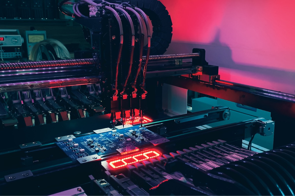
Umieszczanie komponentów: Precyzja i automatyzacja
Dokładne umieszczenie komponentów na PCB jest kamieniem węgielnym montażu SMT. Zadanie to powierza się zaawansowanym maszynom typu pick-and-place, cudom inżynierii, które łączą szybkość, precyzję i elastyczność.
Maszyny typu Pick-and-Place: Rodzaje, możliwości i ograniczenia
Maszyny typu pick-and-place występują w różnych konfiguracjach, z których każda jest dostosowana do konkretnych potrzeb. „Chip shooters” są zoptymalizowane pod kątem szybkiego umieszczania małych, pasywnych komponentów, podczas gdy „elastyczne umieszczarki” obsługują szerszy zakres rozmiarów i kształtów komponentów, w tym układy scalone (IC). Systemy modułowe oferują skalowalność, umożliwiając producentom dodawanie głowic umieszczających w razie potrzeby. Maszyny te charakteryzują się imponującą szybkością umieszczania, często przekraczającą dziesiątki tysięcy komponentów na godzinę. Jednak dokładność jest najważniejsza. Nowoczesne maszyny osiągają dokładność umieszczania do kilkudziesięciu mikrometrów, ale jest to stale kwestionowane przez stale zmniejszający się rozmiar komponentów. Czynniki takie jak kalibracja maszyny, mechanizmy centrowania komponentów i nieodłączna stabilność samej maszyny przyczyniają się do dokładności umieszczania. Nawet najmniejsze wibracje lub niewspółosiowość mogą prowadzić do wad.
Systemy wizyjne i rozpoznawanie znaczników fiducjalnych: Zapewnienie dokładności
Aby osiągnąć wymaganą precyzję, maszyny typu pick-and-place w dużym stopniu polegają na zaawansowanych systemach wizyjnych. Systemy te wykorzystują kamery o wysokiej rozdzielczości i zaawansowane algorytmy do lokalizowania i orientowania komponentów oraz do dokładnej rejestracji PCB. Znaczniki fiducjalne, małe, precyzyjnie zdefiniowane wzory umieszczone na PCB, służą jako punkty odniesienia dla systemu wizyjnego. Maszyna wykorzystuje te znaczniki fiducjalne do kompensacji wszelkich drobnych przesunięć lub zniekształceń na płytce. Istnieją różne rodzaje znaczników fiducjalnych, w tym globalne znaczniki fiducjalne do ogólnej rejestracji płytki i lokalne znaczniki fiducjalne do precyzyjnego wyrównywania komponentów o małym rastrze. Na dokładność systemu wizyjnego wpływają czynniki takie jak warunki oświetleniowe, kontrast między znacznikiem fiducjalnym a powierzchnią płytki oraz złożoność algorytmów przetwarzania obrazu.
Podajniki komponentów: Optymalizacja pod kątem szybkości i niezawodności
Podajniki komponentów są niedocenianymi bohaterami procesu pick-and-place, odpowiedzialnymi za dostarczanie komponentów do głowicy umieszczającej w precyzyjny i terminowy sposób. Podajniki taśmowe i bębnowe są najczęściej stosowane, umieszczając komponenty w oddzielnych kieszeniach w taśmie nośnej. Podajniki tacowe są używane do większych komponentów lub tych, które nie nadają się do pakowania w taśmy i bębny. Podajniki rurowe są używane do komponentów o określonych wymaganiach dotyczących orientacji. Inteligentne podajniki, wyposażone w czujniki i możliwości komunikacyjne, mogą dostarczać informacje w czasie rzeczywistym o dostępności komponentów i statusie podawania, minimalizując przestoje i zapobiegając błędom. Konstrukcja i konserwacja podajników mają kluczowe znaczenie dla zapewnienia niezawodnego podawania komponentów, szczególnie w przypadku bardzo małych lub delikatnych komponentów.
Aplikacja pasty lutowniczej: Krytyczny fundament
Aplikacja pasty lutowniczej jest krytycznym krokiem, który stanowi podstawę niezawodnych połączeń lutowanych. Precyzyjne nałożenie pasty lutowniczej na pola lutownicze PCB zapewnia, że dostępna jest odpowiednia ilość lutu dla każdego połączenia.
Drukowanie szablonowe: Parametry procesu i aspekty materiałowe
Drukowanie szablonowe jest najczęściej stosowaną metodą nakładania pasty lutowniczej. Cienki szablon ze stali nierdzewnej lub niklu z otworami odpowiadającymi polom lutowniczym PCB jest wyrównywany nad płytką. Następnie pasta lutownicza jest przeciskana przez otwory za pomocą rakli, osadzając precyzyjną ilość pasty na każdym polu. Proces drukowania szablonowego jest bardzo wrażliwy na różne parametry, w tym nacisk, prędkość i kąt rakli. Parametry te muszą być starannie kontrolowane, aby zapewnić spójne nakładanie pasty i zapobiec defektom. Grubość szablonu i konstrukcja otworów są również kluczowe. Grubość określa objętość nałożonej pasty, a kształt i rozmiar otworów wpływają na charakterystykę uwalniania pasty. Zaawansowane technologie szablonowe, takie jak szablony stopniowe (o różnej grubości na całej powierzchni szablonu) i szablony elektroformowane (o gładszych ścianach otworów), są stosowane w celu sprostania wyzwaniom związanym z montażem komponentów o małym rastrze i złożonych.
Skład pasty lutowniczej: Reologia, topnik i wielkość cząstek
Pasta lutownicza jest złożonym materiałem, starannie opracowaną mieszaniną proszku stopu lutowniczego, topnika i innych dodatków. Reologia pasty, jej charakterystyka przepływu pod wpływem naprężeń, ma kluczowe znaczenie dla udanego drukowania szablonowego. Pasta musi być wystarczająco lepka, aby zachować swój kształt po wydrukowaniu, ale także łatwo przepływać przez otwory szablonu. Topnik odgrywa istotną rolę w usuwaniu tlenków z wyprowadzeń komponentów i pól lutowniczych PCB, promując zwilżanie i zapewniając silne połączenie metalurgiczne. Rodzaj użytego topnika zależy od konkretnego zastosowania i wymaganego procesu czyszczenia. Rozkład wielkości cząstek lutu również wpływa na wydajność pasty. Mniejsze cząstki oferują lepszą definicję druku w zastosowaniach o małym rastrze, ale mogą być bardziej podatne na utlenianie. Wybór pasty lutowniczej jest krytyczną decyzją, wpływającą zarówno na proces montażu, jak i długoterminową niezawodność produktu.
Typowe wady: Zwarcia, efekt nagrobka i puste przestrzenie
Despite meticulous process control, solder paste printing defects can occur. Bridging, the unwanted connection between adjacent pads, is often caused by excessive paste deposition or poor stencil alignment. Tombstoning, where a component stands up on one end during reflow, can result from uneven paste deposition or imbalances in surface tension. Voids, or air pockets within the solder joint, can compromise the mechanical strength and thermal conductivity of the connection. These defects can arise from various factors, including improper stencil design, incorrect printing parameters, and suboptimal solder paste properties. Detecting and preventing these defects requires a thorough understanding of the underlying causes and the implementation of appropriate corrective actions.
Reflow Soldering: The Art and Science of Thermal Profiles
Reflow soldering is the process of heating the solder paste to melt the solder alloy, forming a permanent metallurgical bond between the component leads and the PCB pads. This seemingly simple process is, in fact, a complex interplay of heat transfer, material science, and precise temperature control.
Convection Reflow: Heat Transfer Mechanisms and Zone Control
Convection reflow ovens are the workhorses of SMT assembly, utilizing forced hot air to heat the PCB and its components. These ovens are typically divided into multiple zones, each with independent temperature control. The PCB travels through the oven on a conveyor belt, experiencing a carefully orchestrated thermal profile. The profile typically consists of four distinct zones: preheat, soak, reflow, and cooling. The preheat zone gradually raises the temperature of the board and components, activating the flux and minimizing thermal shock. The soak zone allows the temperature to equalize across the board, ensuring uniform heating. The reflow zone elevates the temperature above the solder’s melting point, forming the solder joints. Finally, the cooling zone solidifies the solder joints, controlling the cooling rate to minimize stress and optimize the microstructure of the solder. Achieving the optimal thermal profile is a delicate balancing act, requiring careful consideration of the specific components, PCB materials, and solder paste used.
Vapor Phase Reflow: Advantages and Limitations in Specific Applications
Vapor phase reflow offers an alternative to convection heating, utilizing the latent heat of vaporization of a specialized fluid to transfer heat to the PCB. The assembly is immersed in a saturated vapor, which condenses on the cooler surfaces, providing uniform and efficient heating. Vapor phase reflow is particularly advantageous for assemblies with high thermal mass or complex geometries, as it ensures excellent temperature uniformity regardless of component size or placement. It also minimizes oxidation due to the inert vapor environment. However, vapor phase reflow has limitations, including higher equipment and fluid costs, the need for specialized fluids with specific boiling points, and potential for component damage due to rapid heating. Consequently, it is typically used in niche applications where its unique benefits outweigh the drawbacks.
Nitrogen Atmosphere Reflow: Minimizing Oxidation and Enhancing Wetting
Reflow soldering in a nitrogen atmosphere has gained popularity due to its ability to minimize oxidation and improve solder wetting. By replacing the oxygen in the reflow oven with nitrogen, the formation of oxides on the component leads and PCB pads is significantly reduced. This results in cleaner solder joints with improved appearance and potentially enhanced reliability. Nitrogen also influences the surface tension of the molten solder, promoting better wetting and reducing the risk of defects like tombstoning and bridging. The purity level of the nitrogen is a critical factor, with higher purity levels generally yielding better results. While nitrogen reflow adds complexity and cost to the process, the benefits in terms of improved solder joint quality and reduced rework often justify the investment, particularly for high-reliability applications.
Post-Reflow Inspection and Testing: Ensuring Quality and Reliability
The final step in the SMT assembly process is a rigorous inspection and testing regime to ensure the quality and reliability of the assembled boards. This involves a combination of automated optical inspection, X-ray inspection, and electrical testing.
Automated Optical Inspection (AOI): Defect Detection and Classification
Automated Optical Inspection (AOI) systems are sophisticated vision systems that automatically inspect assembled PCBs for a wide range of defects. These systems use high-resolution cameras and advanced image processing algorithms to detect missing components, misalignment, solder bridges, insufficient solder, and other common defects. Different AOI techniques are employed, including template matching (comparing the image to a known good image), pattern recognition (identifying specific features or patterns), and statistical process control (analyzing variations in the image data). The effectiveness of AOI depends on factors such as lighting conditions, camera resolution, and the sophistication of the inspection algorithms. While AOI is highly effective in detecting surface-level defects, it cannot identify hidden defects within solder joints or under components.
X-ray Inspection: Unveiling Hidden Solder Joint Integrity
X-ray inspection provides a crucial window into the internal structure of solder joints, revealing hidden defects that are not visible to optical inspection. X-ray systems generate images based on the differential absorption of X-rays by different materials. Solder, being denser than most other materials on the PCB, absorbs more X-rays and appears darker in the image. This allows for the detection of voids, cracks, insufficient solder, and misalignment within solder joints, particularly for components like Ball Grid Arrays (BGAs) where the connections are hidden beneath the package. Different X-ray techniques exist, including 2D (providing a single projection image), 3D (creating multiple projection images from different angles), and computed tomography (CT), which generates cross-sectional images of the assembly. The choice of technique depends on the specific inspection requirements and the complexity of the assembly.
In-Circuit Testing (ICT) and Functional Testing: Validating Performance
In-Circuit Testing (ICT) and functional testing are electrical tests that verify the electrical connectivity and functionality of the assembled PCB. ICT typically uses a “bed of nails” fixture, a platform with an array of spring-loaded probes that make contact with specific test points on the board. This allows for the measurement of individual component values and the detection of shorts, opens, and other electrical defects. Functional testing, on the other hand, verifies the overall performance of the assembled board by simulating its intended operating environment and applying various input signals. This ensures that the board meets its specified functional requirements. The development of comprehensive test programs and the design of appropriate test fixtures are critical for effective ICT and functional testing.
Materiałyoznawstwo w SMT: Głębsze spojrzenie
The reliability and performance of SMT assemblies are intrinsically linked to the materials used in their construction. From the PCB substrate to the solder alloy and the component packaging, each material plays a critical role.
Printed Circuit Boards (PCBs): Substrate Materials and Surface Finishes
The PCB serves as the foundation for the entire assembly, providing mechanical support and electrical interconnection for the components.
FR-4 and High-Frequency Laminates: Properties and Selection Criteria
FR-4, a glass-reinforced epoxy laminate, is the most widely used PCB substrate material due to its balance of cost, performance, and manufacturability. Its properties, including dielectric constant, loss tangent, and glass transition temperature (Tg), are well-characterized and suitable for a wide range of applications. However, for high-frequency applications, where signal integrity is paramount, specialized high-frequency laminates are employed. These materials, such as PTFE-based laminates (e.g., Rogers materials), exhibit lower dielectric constants and loss tangents, minimizing signal loss and distortion at high frequencies. The choice of laminate material depends on the specific electrical requirements of the application, as well as considerations such as operating temperature, mechanical strength, and cost.
Surface Finishes: HASL, ENIG, OSP, and Their Impact on Solderability
The surface finish applied to the PCB pads plays a crucial role in solderability and long-term reliability. Hot Air Solder Leveling (HASL), a process where the board is dipped in molten solder and then leveled with hot air knives, was traditionally the most common surface finish. However, its uneven surface can pose challenges for fine-pitch component placement. Electroless Nickel Immersion Gold (ENIG), a process that deposits a thin layer of gold over a nickel barrier, offers excellent solderability, a flat surface, and good shelf life. Organic Solderability Preservative (OSP) is a thin, organic coating that provides a solderable surface but has a limited shelf life and is sensitive to handling. Other surface finishes, such as immersion silver and immersion tin, are also used in specific applications. The choice of surface finish depends on factors such as component type, assembly process, cost, and environmental considerations.
Thermal Management in PCB Design: Addressing Heat Dissipation
Thermal management is a critical consideration in PCB design, particularly for high-power components and high-density assemblies. Effective heat dissipation is essential to prevent component overheating and ensure long-term reliability. Thermal vias, plated through-holes that connect different layers of the PCB, provide a path for heat to flow away from components to larger copper areas or heat sinks. Copper planes, large areas of copper on the PCB layers, also aid in heat spreading. Embedded heat spreaders, layers of high thermal conductivity materials within the PCB stack, can further enhance heat dissipation. The design of the PCB layout, including the placement of components and the routing of traces, also influences thermal performance. Simulation tools are often used to model the thermal behavior of the PCB and optimize the design for efficient heat dissipation.
Solder Alloys: Composition, Melting Points, and Mechanical Properties
The solder alloy is the metallurgical glue that holds the SMT assembly together. Its composition, melting point, and mechanical properties are critical for ensuring reliable solder joints.
Lead-Free Solder Alloys: SAC305, SN100C, and Emerging Alternatives
The transition to lead-free solder alloys, driven by environmental and health concerns, has been a major shift in the electronics industry. Tin-silver-copper (SAC) alloys, particularly SAC305 (96.5% Sn, 3.0% Ag, 0.5% Cu), have become the dominant lead-free solders due to their relatively low melting point, good wetting characteristics, and acceptable mechanical properties. SN100C, a tin-copper-nickel-germanium alloy, is another popular choice, offering improved resistance to voiding and better drop shock performance. However, lead-free solders generally have higher melting temperatures than traditional tin-lead solders, requiring adjustments to reflow profiles and potentially increasing thermal stress on components. Research continues into new lead-free alloys with improved properties, such as lower melting points, enhanced reliability, and reduced cost.
Low-Temperature Solders: Applications and Challenges
Low-temperature solders, typically based on bismuth-tin or indium alloys, are used in applications where components are sensitive to the high temperatures of standard reflow processes. These solders offer lower processing temperatures, reducing the risk of thermal damage to sensitive components. They are also employed in step soldering processes, where multiple reflow operations are performed at different temperatures. However, low-temperature solders can have limitations, including lower mechanical strength, increased susceptibility to brittle fracture, and potential compatibility issues with certain surface finishes. Careful consideration must be given to the specific application requirements and the potential trade-offs when selecting low-temperature solders.
Solder Joint Reliability: Factors Influencing Fatigue and Creep
Solder joint reliability is a critical concern, particularly in applications where the assembly is subjected to thermal cycling, mechanical stress, or vibration. Solder joints can fail due to fatigue cracking, creep deformation, or a combination of both. Fatigue is the gradual weakening of the solder joint under cyclic loading, while creep is the slow deformation of the solder under sustained stress at elevated temperatures. The composition of the solder alloy, the microstructure of the solder joint, and the geometry of the joint all influence its reliability. Factors such as the coefficient of thermal expansion (CTE) mismatch between the component and the PCB, the operating temperature range, and the presence of voids or intermetallic compounds can also impact solder joint life. Accelerated testing methods, such as thermal cycling and vibration testing, are used to evaluate solder joint reliability and predict long-term performance.
Component Packaging: From BGAs to QFNs and Beyond
The packaging of electronic components has evolved significantly to meet the demands of miniaturization and increased functionality.
Ball Grid Arrays (BGAs): Package Design, Pitch, and Assembly Considerations
Ball Grid Arrays (BGAs) have become ubiquitous in modern electronics due to their high I/O density and excellent electrical performance. BGAs utilize an array of solder balls on the underside of the package for connection to the PCB, enabling a large number of connections in a small footprint. Different BGA package types exist, including plastic BGAs (PBGAs), ceramic BGAs (CBGAs), and flip-chip BGAs (FCBGAs), each with its own advantages and disadvantages in terms of cost, reliability, and thermal performance. BGA package design parameters, such as ball pitch (the distance between adjacent solder balls), ball diameter, and substrate materials, are critical for successful assembly and long-term reliability. Assembly considerations for BGAs include precise solder paste printing, accurate component placement, and carefully controlled reflow profiling to prevent defects such as bridging, voiding, and head-in-pillow.
3.3.2 Quad Flat No-Leads (QFNs): Thermal Pads and Voiding Issues
Quad Flat No-Leads (QFNs) are another popular package type, known for their small size, low profile, and excellent thermal performance. QFNs have a leadless design, with metal pads on the underside of the package for connection to the PCB. They often feature a large, exposed thermal pad in the center of the package, which provides a direct path for heat dissipation to the PCB. However, this thermal pad can be prone to voiding during reflow, which can compromise thermal performance and reliability. Optimizing stencil design, solder paste selection, and reflow profile are crucial for minimizing voiding in QFNs. Careful attention must be paid to the outgassing pathways for flux volatiles during reflow to prevent the formation of large voids under the thermal pad.
Chip-Scale Packages (CSPs) and Wafer-Level Packages (WLPs): The Drive Towards Miniaturization
Chip-Scale Packages (CSPs) and Wafer-Level Packages (WLPs) represent the leading edge of packaging technology, enabling further miniaturization and integration. CSPs are defined as packages that are no more than 1.2 times the size of the die they contain, while WLPs are fabricated at the wafer level, with the interconnects and final package formed directly on the wafer before dicing. These advanced packages offer significant advantages in terms of size reduction, improved electrical performance due to shorter interconnect lengths, and potential for cost savings through wafer-level processing. However, they also present challenges for assembly, including the need for specialized equipment, tighter process control, and careful handling to prevent damage to the delicate structures.
Wyzwania i niuanse w montażu SMT o wysokiej niezawodności
While SMT has become the dominant assembly technology, certain applications demand even higher levels of reliability and performance. These high-reliability applications, such as those found in aerospace, medical, and automotive industries, push the boundaries of SMT, requiring meticulous attention to detail and a deep understanding of the potential failure mechanisms.
Miniaturization and High-Density Interconnects (HDIs): Pushing the Limits
The relentless drive towards miniaturization has led to the development of High-Density Interconnects (HDIs), PCBs with finer features, smaller vias, and higher component densities than conventional boards.
Microvias and Via-in-Pad Technology: Design and Manufacturing Challenges
Microvias, with diameters typically less than 150 micrometers, are a key enabling technology for HDIs. These tiny vias allow for increased routing density and shorter signal paths, improving electrical performance. However, their fabrication presents significant challenges. Laser drilling and plasma etching are commonly used to create microvias, but ensuring consistent via quality, including clean hole walls and proper plating, requires precise process control. Via-in-pad technology, where microvias are placed directly within the copper pads used for component soldering, further increases routing density but adds complexity to the assembly process. The smaller pad size and the presence of the via within the pad can impact solder paste printing and reflow, requiring careful optimization to prevent defects.
Fine-Pitch Component Assembly: Tolerances and Process Control
High-reliability applications often involve the use of fine-pitch components, where the spacing between adjacent leads or solder balls is extremely small. Assembling these components reliably requires exceptional precision in all aspects of the SMT process. Component placement accuracy becomes even more critical, as even slight misalignments can lead to bridging or open circuits. Solder paste printing must be meticulously controlled to ensure the correct volume of paste is deposited on each pad without bridging. Reflow profiling needs to be carefully optimized to achieve complete solder melting and wetting without causing component damage or exacerbating the risk of bridging. The tolerances on component dimensions, PCB fabrication, and assembly equipment become increasingly tight, demanding a higher level of process control and quality assurance.
Signal Integrity and Electromagnetic Interference (EMI) in HDI Designs
The high component density and fine features of HDI designs can exacerbate signal integrity and electromagnetic interference (EMI) issues. High-speed signals are more susceptible to crosstalk, reflections, and attenuation in HDI boards due to the close proximity of traces and the use of microvias. Careful PCB layout, including impedance control, proper trace routing, and the use of ground planes, is essential to maintain signal integrity. EMI, the unwanted emission or reception of electromagnetic energy, can also be a concern in HDI designs. Shielding, grounding, and filtering techniques may be necessary to mitigate EMI and ensure compliance with electromagnetic compatibility (EMC) standards. Simulation tools play a crucial role in analyzing and optimizing HDI designs for signal integrity and EMI performance.
Thermal Management in High-Power Applications: Dissipating Heat Effectively
High-power applications, where components generate significant amounts of heat, present unique challenges for SMT assembly. Effective thermal management is crucial to prevent component overheating, ensure long-term reliability, and maintain performance.
Heat Sink Design and Attachment: Materials and Interfaces
Heat sinks are often necessary to dissipate heat from high-power components. The design of the heat sink, including its size, shape, fin configuration, and material, must be carefully considered to maximize heat transfer. Aluminum and copper are commonly used heat sink materials due to their high thermal conductivity. The attachment of the heat sink to the component is also critical. Thermal interface materials (TIMs), such as thermal greases or pads, are used to fill the air gaps between the component and the heat sink, reducing thermal resistance and improving heat transfer. The choice of TIM depends on factors such as the required thermal performance, the flatness and surface finish of the mating surfaces, and the assembly process.
Thermal Interface Materials (TIMs): Properties and Application Methods
Thermal interface materials (TIMs) play a crucial role in bridging the microscopic air gaps between the heat-generating component and the heat sink or PCB. These gaps, if left unfilled, would significantly impede heat flow due to the poor thermal conductivity of air. TIMs are designed to conform to the mating surfaces, filling these gaps and providing a continuous path for heat transfer. Various types of TIMs are available, including thermal greases, phase-change materials, thermal pads, and thermally conductive adhesives. Each type has its own set of properties, such as thermal conductivity, compliance (ability to conform to surfaces), bond line thickness (the thickness of the TIM layer after assembly), and outgassing characteristics (the release of volatile compounds over time). The selection of the appropriate TIM depends on the specific application requirements, including the amount of heat to be dissipated, the flatness and surface finish of the mating surfaces, the required bond line thickness, and the operating temperature range. Proper application of the TIM is also crucial to ensure optimal performance. This may involve dispensing the TIM in a specific pattern, applying a controlled pressure during assembly, or using specialized equipment for precise placement.
Active Cooling Solutions: Fans, Liquid Cooling, and Thermoelectric Coolers
In some high-power applications, passive cooling methods, such as heat sinks, may be insufficient to dissipate the heat generated by components. In such cases, active cooling solutions may be necessary. Fans are commonly used to increase airflow over heat sinks, enhancing convective heat transfer. Liquid cooling systems, which circulate a coolant through a heat exchanger attached to the component, offer even higher cooling capacity. Thermoelectric coolers (TECs), also known as Peltier coolers, use the Peltier effect to create a temperature difference between two junctions, actively transferring heat away from the component. The choice of active cooling solution depends on the specific thermal requirements of the application, as well as considerations such as power consumption, noise level, size constraints, and reliability.
Conformal Coating and Encapsulation: Protecting Against Harsh Environments
Aplikacje o wysokiej niezawodności często wymagają, aby zespoły elektroniczne działały w trudnych warunkach, gdzie mogą być narażone na wilgoć, kurz, chemikalia, wibracje i ekstremalne temperatury. Powłoki konforemne i hermetyzacja to dwie popularne metody ochrony zespołów przed tymi czynnikami środowiskowymi.
Materiały na powłoki konforemne: akryle, silikony, uretany i parylen
Powłoki konforemne to cienkie, polimerowe warstwy nakładane na powierzchnię zmontowanej płytki PCB, aby zapewnić barierę przed zanieczyszczeniami środowiskowymi. Dostępne są różne rodzaje materiałów na powłoki konforemne, z których każdy ma swoje unikalne właściwości i charakterystyki wydajności. Powłoki akrylowe są stosunkowo niedrogie i łatwe w aplikacji, oferując dobrą ochronę przed wilgocią i dielektryczną. Powłoki silikonowe zapewniają doskonałą odporność na wysokie temperatury i elastyczność. Powłoki uretanowe oferują dobrą odporność chemiczną i odporność na ścieranie. Powłoki parylenowe, nakładane w procesie osadzania z fazy gazowej, zapewniają bardzo cienką, jednolitą i wysoce konforemną powłokę o doskonałych właściwościach barierowych. Wybór materiału na powłokę konforemną zależy od specyficznych warunków środowiskowych, na jakie będzie narażony zespół, a także od czynników takich jak koszt, łatwość aplikacji i możliwość przeróbki.
Metody aplikacji: natryskiwanie, zanurzanie i powlekanie selektywne
Powłoki konforemne można nakładać różnymi metodami, w tym natryskiwaniem, zanurzaniem, szczotkowaniem i powlekaniem selektywnym. Natryskiwanie jest najpopularniejszą metodą, oferującą dobrą kontrolę nad grubością i pokryciem powłoki. Zanurzanie polega na zanurzeniu całego zespołu w kąpieli materiału powłokowego, zapewniając pełne pokrycie, ale potencjalnie wymagając maskowania obszarów, które nie powinny być pokryte. Szczotkowanie jest odpowiednie do produkcji na małą skalę lub do poprawek. Systemy powlekania selektywnego wykorzystują robotyczne urządzenia dozujące do nakładania powłoki tylko na określone obszary płytki, minimalizując potrzebę maskowania. Wybór metody aplikacji zależy od czynników takich jak złożoność zespołu, wymagana grubość i jednolitość powłoki, wielkość produkcji i koszt.4.3.3 Hermetyzacja i zalewanie: materiały i aspekty procesu
Hermetyzacja i zalewanie zapewniają wyższy poziom ochrony niż powłoka konforemna, całkowicie otaczając zespół elektroniczny w stałym lub żelowym materiale. Zapewnia to lepszą ochronę przed wilgocią, chemikaliami, wstrząsami mechanicznymi i wibracjami. Hermetyzacja zazwyczaj odnosi się do procesu pokrywania zespołu stosunkowo cienką warstwą materiału, podczas gdy zalewanie polega na wypełnieniu całej obudowy zawierającej zespół materiałem hermetyzującym. Do hermetyzacji i zalewania stosuje się różne materiały, w tym żywice epoksydowe, silikony, uretany i akryle. Wybór materiału zależy od specyficznych wymagań aplikacji, takich jak zakres temperatur pracy, wymagany poziom ochrony i pożądane właściwości mechaniczne. Sam proces hermetyzacji lub zalewania musi być również starannie kontrolowany, aby zapewnić całkowite wypełnienie wszystkich pustek, zapobiec tworzeniu się pęcherzyków powietrza i zminimalizować naprężenia na elementach podczas utwardzania.
Nowe trendy i przyszłe kierunki w SMT
Dziedzina montażu SMT stale się rozwija, napędzana stale rosnącymi wymaganiami dotyczącymi miniaturyzacji, wyższej wydajności, zwiększonej funkcjonalności i poprawionej niezawodności. Kilka kluczowych trendów kształtuje przyszłość SMT.
Zaawansowane technologie pakowania: pakowanie 3D i System-in-Package (SiP)
Ograniczenia tradycyjnego pakowania 2D, w którym komponenty są umieszczane obok siebie na jednej płaszczyźnie, napędzają rozwój zaawansowanych technologii pakowania, które umożliwiają integrację pionową.
- Pakowanie 3D: Obejmuje to układanie wielu matryc lub pakietów pionowo i łączenie ich za pomocą technik takich jak przelotki przez krzem (TSV), interposery lub łączenie drutowe. Pakowanie 3D oferuje znaczne korzyści w zakresie zwiększonej gęstości integracji, poprawionej wydajności dzięki krótszym długościom połączeń i zmniejszonemu współczynnikowi kształtu. Stwarza jednak również wyzwania związane z zarządzaniem termicznym, niezawodnością połączeń i złożonością produkcji.
- System-in-Package (SiP): Technologia SiP idzie o krok dalej w integracji, integrując wiele komponentów, takich jak układy scalone, komponenty pasywne, a nawet czujniki, w jednym pakiecie. Takie podejście pozwala na tworzenie wysoce zintegrowanych i kompaktowych systemów elektronicznych o zwiększonej funkcjonalności. Projektowanie i produkcja SiP wymagają zaawansowanych technik umieszczania komponentów, łączenia i hermetyzacji.
Elastyczna i rozciągliwa elektronika: nowe materiały i procesy montażu
Rosnące zainteresowanie elektroniką noszoną, elastycznymi wyświetlaczami i wszczepialnymi urządzeniami medycznymi napędza rozwój elastycznej i rozciągliwej elektroniki. Aplikacje te wymagają nowych materiałów i procesów montażu, które mogą wytrzymać zginanie, rozciąganie i wyginanie bez pogarszania wydajności lub niezawodności.
- Nowe materiały: Opracowywane są przewodzące tusze, rozciągliwe podłoża (np. elastomery) i organiczne półprzewodniki, aby umożliwić wytwarzanie elastycznych i rozciągliwych obwodów.
- Procesy montażu: Techniki drukowania, takie jak drukowanie atramentowe i sitodruk, są dostosowywane do wytwarzania elastycznych obwodów. Drukowanie transferowe, w którym elementy obwodu są wytwarzane na sztywnym podłożu, a następnie przenoszone na elastyczne podłoże, jest kolejnym obiecującym podejściem.
Automatyzacja i Przemysł 4.0: inteligentne fabryki i optymalizacja oparta na danych
Rosnąca złożoność montażu SMT oraz potrzeba wyższej produktywności i jakości napędzają wdrażanie automatyzacji i zasad Przemysłu 4.0 w produkcji elektroniki.
- Inteligentne fabryki: Koncepcja „inteligentnej fabryki”, w której maszyny, procesy i systemy są połączone i komunikują się ze sobą, zyskuje na popularności w montażu SMT. Umożliwia to monitorowanie produkcji w czasie rzeczywistym, optymalizację procesów opartą na danych i konserwację predykcyjną.
- Optymalizacja oparta na danych: Ogromne ilości danych generowanych przez sprzęt SMT i systemy kontroli można wykorzystać do poprawy kontroli procesu, redukcji wad i zwiększenia wydajności. Algorytmy uczenia maszynowego można wykorzystać do analizy tych danych, identyfikacji wzorców i optymalizacji parametrów procesu w czasie rzeczywistym.
Zrównoważony rozwój w produkcji elektroniki: zmniejszenie wpływu na środowisko
Przemysł elektroniczny stoi w obliczu rosnącej presji na zmniejszenie swojego wpływu na środowisko. Obejmuje to minimalizację e-odpadów, zmniejszenie zużycia energii i stosowanie bardziej zrównoważonych materiałów.
- Lutowanie bezołowiowe: Przejście na lutowanie bezołowiowe jest znaczącym krokiem w kierunku ograniczenia stosowania niebezpiecznych materiałów w produkcji elektroniki.
- Sprzęt energooszczędny: Producenci opracowują bardziej energooszczędny sprzęt SMT, taki jak piece rozpływowe z ulepszoną izolacją i systemami odzyskiwania ciepła.
- Recykling i gospodarka odpadami elektronicznymi: Podejmowane są wysiłki w celu poprawy recyklingu komponentów elektronicznych i zmniejszenia ilości odpadów elektronicznych trafiających na składowiska.
Wnioski: Stale ewoluujący krajobraz montażu SMT
Technologia montażu powierzchniowego (SMT) zrewolucjonizowała produkcję elektroniki, umożliwiając rozwój mniejszych, lżejszych, mocniejszych i bardziej zaawansowanych urządzeń elektronicznych. Podróż od montażu przewlekanego do SMT charakteryzowała się ciągłymi innowacjami w materiałach, procesach i sprzęcie. Jak zbadaliśmy w tej dogłębnej analizie, podstawowe zasady montażu SMT, od umieszczania komponentów po lutowanie rozpływowe, są złożoną interakcją precyzji, automatyzacji i skrupulatnej kontroli procesu.
Materiały naukowe stanowiące podstawę SMT są równie krytyczne, a właściwości podłoży PCB, stopów lutowniczych i opakowań komponentów odgrywają istotną rolę w niezawodności i wydajności końcowego zespołu. Aplikacje o wysokiej niezawodności przesuwają granice SMT, wymagając jeszcze większej dbałości o szczegóły i głębszego zrozumienia potencjalnych mechanizmów awarii. Miniaturyzacja, połączenia o dużej gęstości, zarządzanie termiczne i ochrona środowiska to tylko niektóre z wyzwań, którym należy sprostać w tych wymagających zastosowaniach.
Przyszłość montażu SMT rysuje się w jasnych barwach, dzięki ciągłemu postępowi w zakresie zaawansowanych opakowań, elastycznej i rozciągliwej elektroniki, automatyzacji i zrównoważonego rozwoju. Trendy te kształtują nową erę produkcji elektroniki, w której inteligentne fabryki, optymalizacja oparta na danych i praktyki przyjazne dla środowiska staną się coraz ważniejsze. W miarę postępów dalsze badania i rozwój w zakresie materiałów, procesów i sprzętu będą niezbędne, aby sprostać stale rosnącym wymaganiom przemysłu elektronicznego. Podróż SMT jeszcze się nie skończyła; to ciągła ewolucja, napędzana nieustannym dążeniem do innowacji i pragnieniem tworzenia coraz potężniejszych i bardziej zaawansowanych systemów elektronicznych, które ukształtują świat jutra.