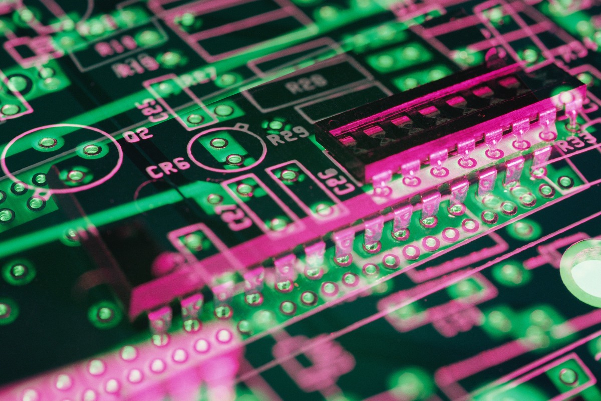
A PCB is a thin board made of insulating material, such as fiberglass or epoxy resin, with conductive pathways etched or printed onto its surface. These pathways, known as traces, are typically made of copper and serve as the electrical connections between various electronic components, such as resistors, capacitors, and integrated circuits. PCBs provide a stable and organized platform for mounting and interconnecting these components, enabling them to work together to perform specific tasks within an electronic device.
The primary function of PCBs is to minimize wiring complexity and improve electronic device reliability. Using a PCB, designers can create compact and efficient circuits that are less prone to errors and easier to troubleshoot. PCBs have become an integral part of virtually all electronic devices, and their development has been crucial in driving technological advancements across various industries.
This article will explore the rich history of PCBs, spanning over a century, from their earliest concepts to the groundbreaking innovations that have shaped modern electronics. We will examine the key milestones, technological advancements, and the impact of PCBs on our digital world.
Early Concepts and Precursors to PCBs (1900-1940s)
Before the advent of PCBs, electronic devices relied on point-to-point wiring, which involved manually connecting components using individual wires. This method was time-consuming, prone to errors, and resulted in bulky and unreliable devices. The limitations of early electronics drove the need for a more efficient and compact solution, setting the stage for the development of PCBs.
One of the earliest precursors to PCBs was Albert Hanson’s 1903 patent for a flat foil conductor on an insulating board. Hanson’s design featured through-hole construction and conductors on both sides, resembling modern plated through-hole PCBs. In 1925, Charles Ducas patented “printed wiring,” a process that involved using conductive inks to create electrical pathways on an insulated surface.
However, it was Paul Eisler, an Austrian inventor, who developed the first modern PCB concept in the 1930s. Eisler’s design involved etching circuits onto copper foil laminated onto a non-conductive substrate, such as glass. In 1936, he created the first PCB for a radio set, demonstrating the potential of this new technology.
Despite these early innovations, the widespread adoption of PCBs was hindered by the Great Depression and the limitations of manufacturing processes at the time. It would take the demands of World War II to catalyze the further development and application of PCB technology.
World War II and Military Applications (1940s)
The outbreak of World War II drove the need for more advanced and reliable electronics, particularly in military applications. PCBs played a crucial role in meeting these demands, offering improved reliability, reduced size, and the potential for mass production.
During the war, one of the most significant applications of PCBs was in proximity fuses for artillery shells and bombs. These fuses required compact and robust electronic circuits that could withstand the extreme conditions of military use. In collaboration with the British, the U.S. military adopted and further developed PCB technology to produce these fuses on a large scale.
In 1943, Paul Eisler made another significant contribution by developing a PCB-equipped radio. This innovation demonstrated the potential of PCBs in complex electronic devices and paved the way for future military applications.
The advantages of PCBs, such as their reliability, size reduction, and suitability for mass production, made them invaluable to the war effort. The military’s adoption and refinement of PCB technology during this period laid the foundation for their widespread commercial use in the decades that followed.
Commercialization and Widespread Adoption (1950s-1960s)
Following World War II, PCB technology was released for commercial use in 1948. This marked the beginning of a new era in electronics, as PCBs began to be incorporated into a wide range of consumer products.
The 1950s saw the introduction of transistors, which revolutionized the electronics industry by enabling smaller and more reliable devices. The combination of transistors and PCBs allowed for the development of compact and efficient electronic products, such as radios and televisions.
During this period, PCBs evolved from single-sided boards to double-sided designs, with components on one side and identification printing on the other. The use of materials like zinc plates and corrosion-resistant coatings further improved the durability and reliability of PCBs.
The 1960s brought another significant advancement with the introduction of integrated circuits (ICs) or silicon chips. ICs allowed for the miniaturization of electronic components, with thousands of components placed on a single chip. PCBs had to evolve to accommodate these new components, incorporating more layers and smaller form factors.
The commercialization and widespread adoption of PCBs in the 1950s and 1960s were driven by the demands of various industries, including consumer electronics, telecommunications, and aerospace. As PCBs became more sophisticated and reliable, they enabled the development of increasingly complex and powerful electronic devices, setting the stage for the future digital revolution.
Technological Advancements (1970s-1990s)
From the 1970s to the 1990s, we witnessed significant technological advancements in PCB design and manufacturing, driven by the increasing demands for smaller, faster, and more reliable electronic devices.
In the 1970s, the introduction of solder masks greatly improved the reliability and manufacturability of PCBs. Solder masks are thin layers of polymer applied to the surface of the PCB, protecting the copper traces from oxidation and preventing solder bridges between closely spaced components.
The 1980s saw the development of surface mount technology (SMT), which revolutionized PCB assembly by allowing components to be mounted directly onto the surface of the board without the need for through-hole connections. SMT enabled the production of smaller, more densely packed PCBs, further driving the trend towards miniaturization.
The 1990s focused on increased miniaturization and the use of computer-aided design (CAD) in PCB development. High-density interconnect (HDI) technology emerged, enabling the creation of PCBs with finer traces and smaller vias, allowing for even greater component density.
The adoption of CAD software streamlined the PCB design process, allowing for more complex and optimized layouts. CAD tools enabled designers to create and simulate PCBs virtually, reducing the time and cost of physical prototyping.
These technological advancements significantly improved PCB performance, reliability, and manufacturing efficiency. They enabled the development of increasingly sophisticated electronic devices, from personal computers and mobile phones to medical equipment and aerospace systems, paving the way for the digital age.
Modern PCB Developments (2000s-Present)
In the 21st century, PCB technology has continued to evolve, driven by the ever-increasing demands for smaller, faster, and more powerful electronic devices. Modern PCB developments have focused on advanced materials, manufacturing processes, and integration with emerging technologies.
One of the most significant advancements has been the development of multi-layer and flexible PCBs. Multi-layer PCBs, with their ability to accommodate a higher density of components and connections, have become essential for complex electronic devices. Flexible PCBs, made from materials like polyimide, have enabled the creation of bendable and wearable electronics, opening up new possibilities for product design.
High-density interconnect (HDI) technology has continued to advance, allowing for even finer traces and smaller vias. This has been crucial for the development of compact, high-performance devices like smartphones, smartwatches, and IoT sensors.
De integratie van PCB's met opkomende technologieën, zoals het Internet of Things (IoT), kunstmatige intelligentie (AI) en 5G-netwerken, is steeds belangrijker geworden. PCB's die zijn ontworpen voor deze toepassingen, moeten voldoen aan strenge eisen voor snelle gegevensoverdracht, lage latentie en energie-efficiëntie.
Vooruitgang in PCB-materialen en productieprocessen is ook significant geweest. Geavanceerde substraten, zoals hoogfrequente laminaten en metalen kern-PCB's, hebben de signaalintegriteit en het thermisch beheer verbeterd. De adoptie van 3D-printtechnologie heeft het mogelijk gemaakt om snel prototypes te maken en complexe PCB-structuren te produceren.
Naarmate de vraag naar duurzame en milieuvriendelijke producten groeit, heeft de PCB-industrie zich ook gericht op de ontwikkeling van milieuvriendelijke materialen en processen. Dit omvat het gebruik van loodvrije soldeer, halogeenvrije laminaten en recyclebare substraten.
Moderne PCB-ontwikkelingen hebben de evolutie van elektronische apparaten mogelijk gemaakt, van consumentengadgets tot industriële automatiseringssystemen. Naarmate de technologie vordert, zullen PCB's ongetwijfeld een cruciale rol spelen bij het vormgeven van de toekomst van de elektronica.
Impact en betekenis van PCB's
De impact en betekenis van PCB's in de moderne wereld kan niet genoeg worden benadrukt. Deze bescheiden printplaten zijn de stille aanjagers van de digitale revolutie geweest en hebben de manier waarop we leven, werken en communiceren veranderd.
Een van de belangrijkste bijdragen van PCB's is hun rol in het mogelijk maken van de miniaturisatie van elektronische apparaten. Het compacte en efficiënte ontwerp van PCB's heeft de ontwikkeling mogelijk gemaakt van steeds kleinere en krachtigere apparaten, van smartphones en laptops tot medische implantaten en draagbare technologie. Deze miniaturisatie heeft elektronica toegankelijker, draagbaarder en geïntegreerder in ons dagelijks leven gemaakt.
PCB's zijn cruciale componenten in verschillende industrieën, waaronder consumentenelektronica, ruimtevaart, auto-industrie en medische apparatuur. In de ruimtevaartindustrie zijn PCB's essentieel voor de betrouwbare werking van avionica, communicatiesystemen en satelliettechnologie. In de automobielsector maken PCB's de werking mogelijk van motorregeleenheden, infotainment systemen en geavanceerde bestuurdersassistentiesystemen (ADAS). In de medische sector zijn PCB's cruciaal voor de ontwikkeling van diagnostische apparatuur, bewakingsapparatuur en levensondersteunende systemen.
PCB's hebben ook bijgedragen aan belangrijke technologische vooruitgang en verbeterde productbetrouwbaarheid. De standaardisatie en automatisering van PCB-productieprocessen hebben de massaproductie mogelijk gemaakt van hoogwaardige elektronische apparaten met consistente prestaties en lagere uitvalpercentages. Dit heeft geleid tot de wijdverbreide beschikbaarheid van betaalbare en betrouwbare consumentenelektronica, evenals de ontwikkeling van missiekritieke systemen in industrieën zoals de ruimtevaart en defensie.
De productie en verwijdering van PCB's hebben echter ook milieu- en gezondheidsproblemen veroorzaakt. Het gebruik van gevaarlijke materialen, zoals lood en gehalogeneerde verbindingen, in de traditionele PCB-productie heeft geleid tot problemen met elektronisch afval en potentiële gezondheidsrisico's voor werknemers en gemeenschappen. Als reactie hierop werkt de industrie aan de ontwikkeling en adoptie van duurzamere en milieuvriendelijkere materialen en processen.
De economische impact van de PCB-industrie is significant, met een wereldwijde marktwaarde die naar verwachting $89,7 miljard zal bereiken in 2024. De industrie ondersteunt een enorm ecosysteem van fabrikanten, leveranciers en ontwerpers, waardoor banen worden gecreëerd en innovatie in meerdere sectoren wordt gestimuleerd. Naarmate de vraag naar elektronische apparaten groeit, staat de PCB-industrie klaar voor verdere expansie en technologische vooruitgang.
Conclusie
Gedurende hun reis hebben PCB's de manier veranderd waarop we elektronische apparaten ontwerpen, produceren en gebruiken. Ze hebben de miniaturisatie van elektronica mogelijk gemaakt, de betrouwbaarheid en prestaties verbeterd en nieuwe mogelijkheden voor innovatie in verschillende industrieën geopend. Van de vroege militaire toepassingen tijdens de Tweede Wereldoorlog tot de moderne wonderen van smartphones, IoT-apparaten en ruimtevaartsystemen, PCB's zijn de ruggengraat van de technologische vooruitgang geweest.
Als we naar de toekomst kijken, blijft de rol van PCB's bij het vormgeven van het elektronische landschap even cruciaal als altijd. De voortdurende ontwikkeling van geavanceerde materialen, productieprocessen en integratie met opkomende technologieën zal de volgende generatie elektronische apparaten aandrijven.