Desain PCB
Buka Potensi Inovasi dengan Layanan Desain PCB Mutakhir kami
Desain PCB
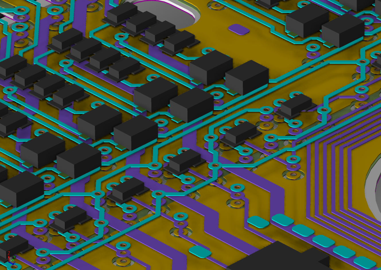
Desain PCB adalah proses menciptakan tata letak dan pengaturan komponen elektronik pada PCB. Langkah penting dalam proses manufaktur ini melibatkan penerjemahan diagram skematik sirkuit ke dalam desain fisik yang dapat diproduksi dan dirakit. Tim desainer kami yang terampil dan berpengalaman menggunakan perangkat lunak dan alat desain terbaru untuk memastikan desain PCB yang akurat dan efisien. Dengan perhatian yang tajam terhadap detail dan fokus pada fungsionalitas, kami bertujuan untuk membuat desain PCB yang dioptimalkan untuk kinerja, keandalan, dan kemampuan manufaktur. Apakah Anda memerlukan desain lapisan tunggal yang sederhana atau desain multilayer yang rumit, kami memiliki keahlian untuk memberikan desain PCB berkualitas tinggi yang memenuhi kebutuhan spesifik Anda.

Di Bester, kami bangga memberikan layanan Desain PCB terbaik kepada pelanggan kami yang berharga. Dengan tim desainer yang sangat terampil dan berpengalaman, kami memastikan bahwa setiap proyek dibuat dengan cermat untuk memenuhi persyaratan dan spesifikasi unik klien kami. Perangkat lunak desain mutakhir dan teknologi canggih kami memungkinkan kami membuat desain PCB yang sangat efisien dan inovatif yang dioptimalkan untuk kinerja, keandalan, dan efektivitas biaya. Kami bekerja sama dengan pelanggan kami selama proses desain, menyediakan komunikasi dan umpan balik yang konstan untuk memastikan harapan mereka terlampaui. Baik itu desain multi-layer yang kompleks atau papan lapisan tunggal yang sederhana, kami memiliki keahlian dan sumber daya untuk memberikan solusi Desain PCB yang luar biasa yang memenuhi standar industri tertinggi. Percayai Bester untuk semua kebutuhan Desain PCB Anda dan rasakan perbedaan kualitas dan keunggulannya.
KEMAMPUAN LAYANAN DESAIN PCB
Pengambilan Skema
Kami dapat membuat skema dari spesifikasi, lembar skematik yang sudah ditandai, atau diagram hitam dan diskusi verbal. Kami menerima skema dalam format apa pun (PDF, sketsa, dll.) dan dapat mengonversinya ke dalam format CAD yang diinginkan. Sebagai bagian dari proses kami, kami memvalidasi BOM.
Rekayasa Balik
Kita dapat mengambil papan yang sudah ada dari papan kosong, papan rakitan, file desain dan gambar yang sudah ada. Dan kita dapat membuat desain baru dengan semua dokumentasi pendukung.
Optimalisasi Biaya
Kami dapat meninjau produk atau desain yang sudah ada dan mengusulkan metode untuk pengurangan biaya. Dalam banyak kasus, pengurangan lapisan dapat dicapai dengan menggunakan geometri yang lebih kecil untuk konduktor dan vias serta penggunaan mikrovias yang dibor dengan laser.
Desain Tumpukan PCB
Sebelum memulai desain tata letak, kami akan melakukan desain susunan in-house sehingga semua tujuan desain terpenuhi. Kami juga akan menyarankan apakah teknologi HDI diperlukan atau dapat membantu dalam pengoptimalan PCB.
Alat Desain PCB
Kami menggunakan alat standar dari Cadence, Mentor Graphics dan Altium. Kami dapat menerima netlist atau netlist yang ditempatkan sebagian / seluruhnya. Kami dapat menggunakan perpustakaan suku cadang kami atau perpustakaan pelanggan. Kami dapat menyediakan. Layanan 24/7 dan tim desain kami dapat menjadwalkan konferensi video untuk mendukung Anda. Kami memiliki akses ke sumber daya di luar negeri yang dapat mengerjakan desain Anda saat Anda tidur.
Layanan Integritas Sinyal
Kami dapat melakukan layanan integritas sinyal pada desain papan kecepatan tinggi apa pun yang kami buat. Kami akan menangani persyaratan impedansi kontrol dan crosstalk; kami akan menangani bahan PCB yang sesuai untuk mencapai serangkaian spesifikasi integritas sinyal yang diberikan.
Kemampuan Desain PCB
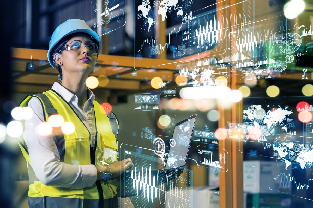
Sebagai produsen PCB dan perakitan profesional, kami memiliki pemahaman yang lebih baik tentang cara merancang papan PCB yang dapat diproduksi, andal, dan hemat biaya daripada pemasok lain.
Di Bester Tech, Anda dapat menikmati layanan solusi PCB satu atap mulai dari desain PCB, pembuatan PCB hingga prototipe jadi dan perangkat perakitan PCB bervolume tinggi. Metodologi teknik kami yang matang memastikan desain yang efisien dan hemat biaya, dilakukan dengan benar pada kali pertama.
Kami menawarkan 2 tahap tinjauan desain, baik secara offline maupun online interaktif. Desain PCB dapat disediakan dengan menggunakan perangkat lunak desain PCB standar industri:
- PERANGKAT LUNAK DESAIN
-
- PADS (Mentor Graphics)
- Irama (ORCAD & Allegro)
- Desainer Altium (Altium)
- LAYANAN YANG DISEDIAKAN
-
- Kami dapat mengambil skema dalam bentuk apa pun (pdf, sketsa, dll.) dan mengonversinya ke dalam format CAD elektronik yang tepat.
- Aturan desain yang dikomunikasikan pada tingkat skema.
- Desain tapak khusus untuk memenuhi kebutuhan Anda.
- BOM dan harga komponen yang bersaing untuk setiap desain.
- Gambar Fabrikasi, Perakitan, dan file Gerber untuk memenuhi persyaratan manufaktur.
- PCB yang kaku/fleksibel; bentuk papan yang kompleks dapat dibuat.
- PENGIRIMAN
-
- Gambar Skema Lengkap
- Gambar tumpukan lapisan PCB.
- Lengkapi file PDF 3D
- File fabrikasi (Format standar adalah Gerber Extended; Gerber X2, ODB++, IPC-2581 tersedia berdasarkan permintaan)
- File Rute dan Bor
- Gambar perakitan
- Pilih dan Tempatkan file (Data Centroid)
- Spesifikasi fabrikasi (Tumpukan Lapisan, Meja Bor dan Gambar, dll.)
- Daftar lengkap Bill of Material (BOM)
- Output lain yang ditentukan pelanggan
Mengapa Memilih Bester

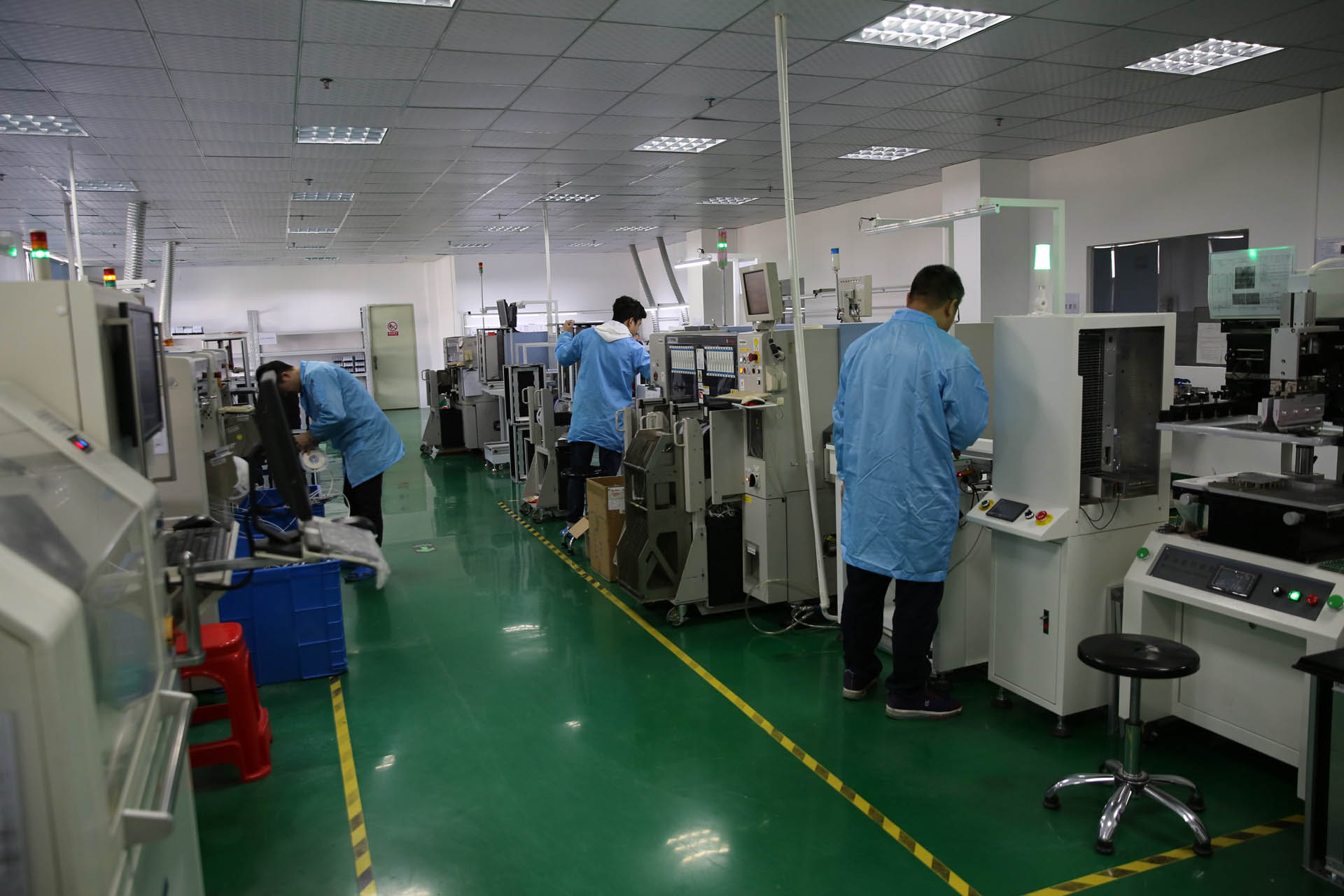
Kapasitas Perakitan yang Kuat
Dengan fasilitas canggih dan tim yang sangat terampil, kami memiliki kapasitas untuk menangani proyek perakitan PCB yang paling rumit sekalipun, memastikan produk Anda diproduksi secara efisien dan akurat.

Jaminan Kualitas
Proses kontrol kualitas kami yang ketat dan prosedur pengujian ekstensif menjamin bahwa setiap perakitan PCB yang kami produksi memenuhi standar industri tertinggi untuk keandalan dan kinerja, memberi Anda ketenangan pikiran dan kepercayaan diri dalam layanan kami.

Layanan Satu Atap
Dari fabrikasi dan desain PCB hingga sumber komponen dan pemrograman IC, Bester menawarkan berbagai layanan yang komprehensif di bawah satu atap, merampingkan proses produksi dan menghemat waktu dan tenaga Anda.

Perputaran Cepat
Komitmen kami terhadap waktu penyelesaian yang cepat berarti bahwa proyek perakitan PCB Anda akan selesai sesuai jadwal, sehingga Anda dapat memenuhi tenggat waktu produksi dan membawa produk Anda ke pasar dengan cepat.
Klien dan Sertifikasi

Kemampuan Manufaktur Elektronik di Bester
Kemampuan Manufaktur
- Kontrol Komponen ESD 100%
- 8 Jalur SMT
- 4 Garis DIP
- 40 Penyolderan Robot Otomatis
- Mesin CNC
- Pelapisan Konformal Otomatis
- Cetakan Injeksi
- Pencetakan 3D
Sertifikasi
- ISO 9001
- UL
- SGS
- IPC
- RoHS
- CE
- FCC
- SRDI (Perusahaan "Khusus, Penyempurnaan, Diferensial, Inovasi" Tiongkok)
- HNTE (Perusahaan Teknologi Tinggi dan Baru Tiongkok)
Industri yang Kami Layani
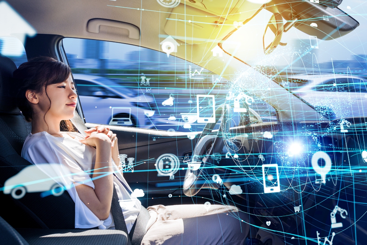
Otomotif
Kami memahami peran penting PCBA dalam industri otomotif. Dengan layanan PCBA kami yang komprehensif, kami memenuhi kebutuhan spesifik produsen otomotif, membantu mereka menghadirkan sistem elektronik yang andal dan berkinerja tinggi.
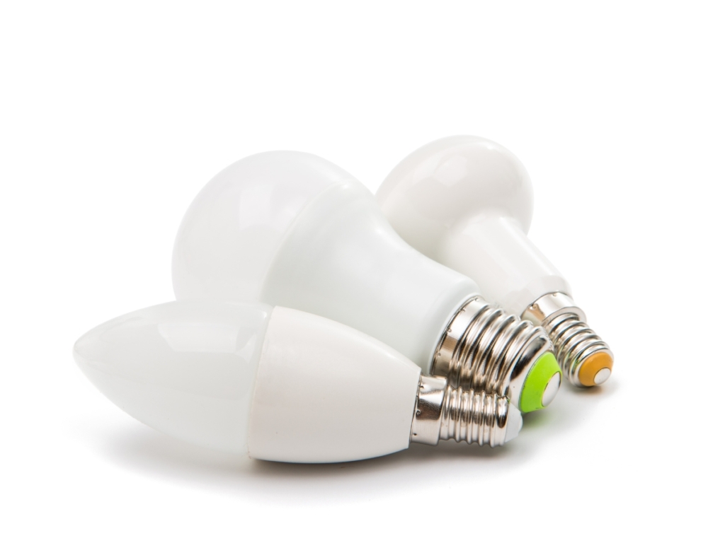
LED
Di pasar LED, Bester menyediakan solusi PCBA terbaik yang sangat penting untuk produksi produk pencahayaan LED berkualitas tinggi. Kami bekerja sama dengan produsen LED untuk memastikan bahwa PCBA mereka memenuhi persyaratan ketat efisiensi energi, daya tahan, dan kinerja.
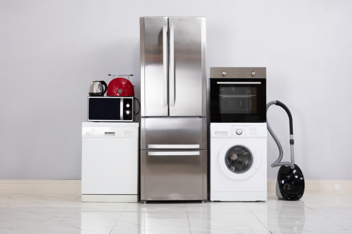
Elektronik Konsumen
Bester melayani pasar elektronik konsumen dengan menawarkan berbagai layanan PCBA yang memungkinkan produksi perangkat elektronik yang inovatif dan ramah pengguna. Kami berkolaborasi dengan produsen elektronik konsumen untuk memastikan bahwa PCBA mereka memenuhi standar kualitas dan fungsionalitas tertinggi.
Industri
Di sektor industri, layanan PCBA Bester memainkan peran penting dalam pengembangan sistem elektronik yang andal dan efisien. Kami bekerja sama dengan produsen peralatan industri untuk memenuhi persyaratan khusus mereka, memastikan bahwa PCBA kami dapat bertahan dalam kondisi lingkungan yang keras dan memberikan kinerja yang optimal.
APLIKASI PCBA
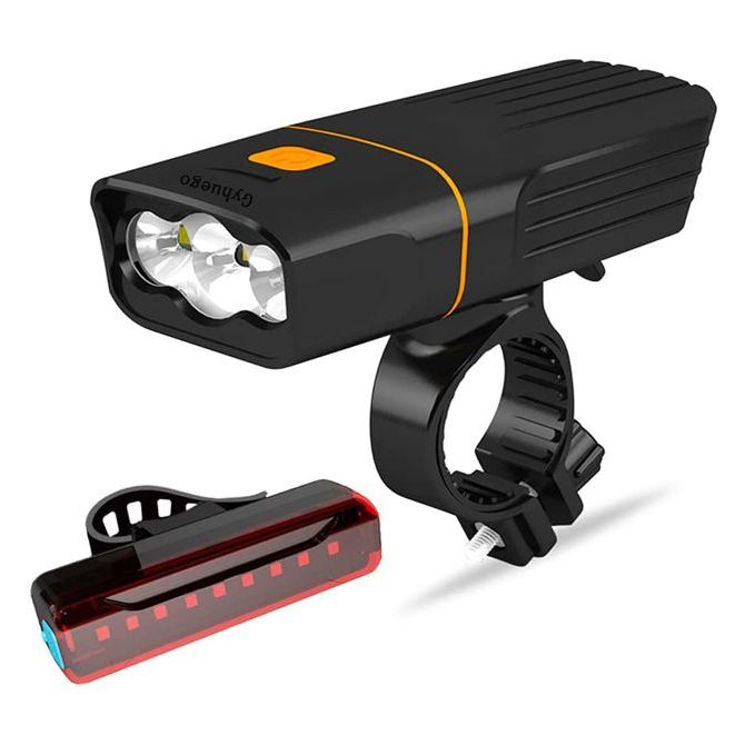
PCBA Lampu Sepeda
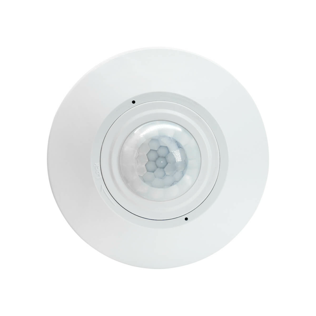
Sensor Gerak PIR PCBA
PCBA LED
Tanya Jawab Perakitan PCB
Apakah Anda produsen PCB bersertifikat?
Proses bahan aditif, juga dikenal sebagai manufaktur aditif, melibatkan 123444412312312321on, seperti printhead yang dipanaskan atau laser, untuk mengikat lapisan-lapisan menjadi satu. Replika yang persis sama dengan model aplikasi peleburan 3D asli.
Apakah Anda produsen PCB bersertifikat?
Proses bahan aditif, juga dikenal sebagai manufaktur aditif, melibatkan penggunaan printer 3D untuk membuat objek padat dari model 3D. Proses ini memerlukan penambahan bahan atau filamen lapis demi lapis, dan kemudian menggunakan aplikasi peleburan, yaitu aplikasi peleburan, yaitu aplikasi peleburan, yaitu aplikasi peleburan, yaitu aplikasi peleburan, yaitu aplikasi peleburan, yaitu aplikasi peleburan, yaitu aplikasi peleburan, yaitu printhead atau laser yang dipanaskan, untuk mengikat lapisan-lapisan tersebut menjadi satu. Hasil akhirnya adalah objek cetakan 3D yang merupakan replika persis model 3D aslinya.
Apakah Anda produsen PCB bersertifikat?
Proses bahan aditif, juga dikenal sebagai manufaktur aditif, melibatkan penggunaan printer 3D untuk membuat objek padat dari model 3D. Proses ini memerlukan penambahan bahan atau filamen lapis demi lapis, dan kemudian menggunakan aplikasi peleburan, seperti printhead yang dipanaskan atau laser, untuk mengikat lapisan-lapisan tersebut. Hasil akhirnya adalah objek cetak 3D yang merupakan replika persis dari model 3D asli.
Apakah Anda menawarkan layanan PCBA giliran cepat?
Proses bahan aditif, juga dikenal sebagai manufaktur aditif, melibatkan penggunaan printer 3D untuk membuat objek padat dari model 3D. Proses ini memerlukan penambahan bahan atau filamen lapis demi lapis, dan kemudian menggunakan aplikasi peleburan
Apakah Anda menerima pesanan dalam jumlah kecil?
Proses bahan aditif, juga dikenal sebagai manufaktur aditif, melibatkan aplikasi peleburan, aplikasi peleburan, aplikasi peleburan, aplikasi peleburan, aplikasi peleburan, aplikasi peleburan, aplikasi peleburan, aplikasi peleburan, melibatkan penggunaan printer 3D untuk membuat objek padat dari model 3D. Proses ini memerlukan penambahan bahan atau filamen lapis demi lapis, dan kemudian menggunakan aplikasi peleburan, seperti printhead yang dipanaskan atau laser, untuk mengikat lapisan-lapisan tersebut. Hasil akhirnya adalah objek cetak 3D yang merupakan replika persis dari model 3D asli.

Siap Memulai Proyek Perakitan PCB Anda?