Pengujian Fungsional
Unlock the full potential of your electronic devices with Bester’s advanced Functional Testing services.
Pengujian Fungsional
Functional Testing is a crucial aspect of our comprehensive range of services at Bester. As a leading PCBA manufacturer, we understand the importance of ensuring that every electronic component and circuit board functions flawlessly. Functional Testing is a meticulous process that involves evaluating the performance and functionality of a product, verifying that it meets the required specifications and performs as intended. Our team of skilled technicians and engineers meticulously conduct a series of tests, using advanced equipment and techniques, to identify any potential defects or issues. By conducting Functional Testing, we ensure that our customers receive products of the highest quality and reliability, meeting their specific requirements and industry standards.

At Bester, we understand the importance of ensuring the functionality and reliability of your printed circuit boards (PCBs). That’s why we offer top-notch Functional Testing services to meet your specific requirements. Our experienced team of technicians and engineers utilize advanced testing equipment and methodologies to thoroughly assess the functionality of your PCBs. From performing in-circuit tests to functional tests, we meticulously evaluate each component and circuit to identify any potential faults or issues. By conducting comprehensive Functional Testing, we help you minimize the risk of defects and ensure the highest level of quality and performance for your PCBs. Trust Bester for reliable and accurate Functional Testing services that guarantee the functionality and reliability of your PCBs.
Functional Testing Capabilities
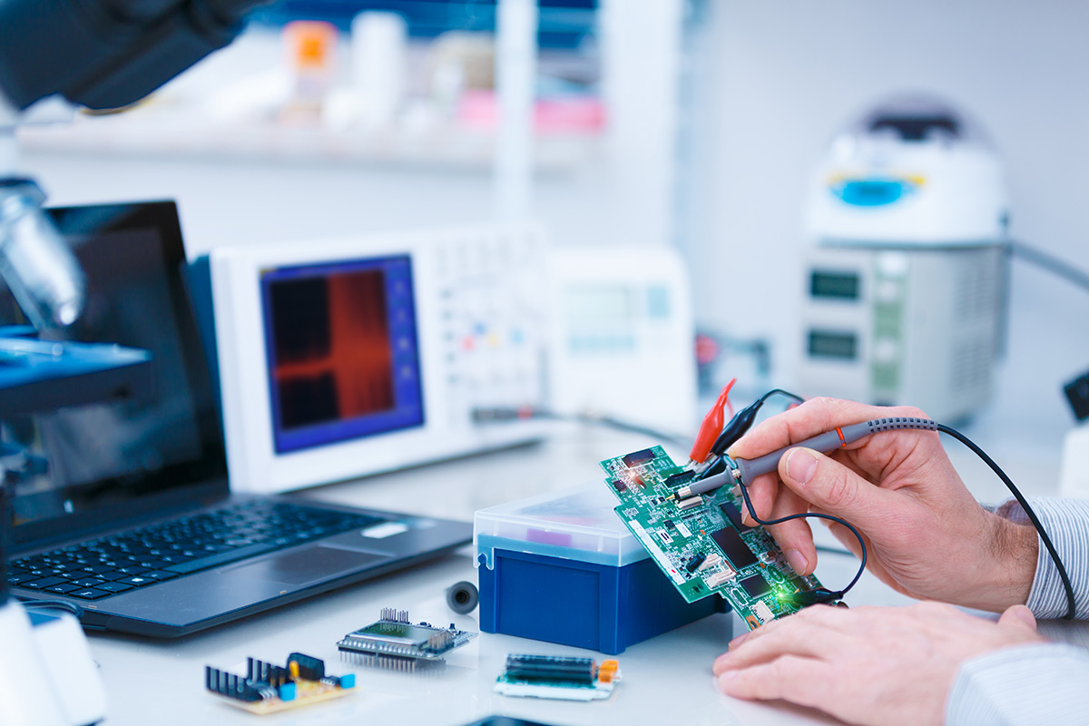
FCT is performed through a combination of connecting a cable to your PCBs on-board connectors, and the use of test probes contacting test points where necessary on your board. The testing software for the board is developed to conduct the tests per the specific requirements of the board’s function.
The goal of the functional test is to look at your entire PCB assembly and its functionality to determine whether or not it has been manufactured according to your specifications. This requires a reliable EMS (electronic manufacturing service) provider who knows how to best work with your PCB assembly for testing.
- Functional types of PCB testing include
- X-ray inspection
- Micro-sectioning analysis
- PCB contamination test
- PCB solderability test
- Time-domain reflectometer testing (TDR)
- Peel test
- Solder float test
ADDITIONAL INFORMATION
How to Perform Functional Testing?
Functional testing is performed in the last step of PCB assembly manufacturing process. A functional test emulates the operational environment to ensure the PCBA’s correct functionality. The operational environment may consist of a device that communicates with the PCBA DUT. Typically, the DUT’s power supply and software test program will load the necessary parameters to make the DUT work properly.
Functional testing will verify the functionality of your PC board assembly. It will do this by applying a range of different signals and currents to stimulate the board’s behavior based on testing software developed for the board, and then measure how the PCBA reacts. It will detect both analog and digital signal problems, including distortions, incorrect currents, and signal timing issues.
The printed circuit board assembly (PCBA) may be subjected to a sequence of signals and power supply voltages. Responses are monitored at specific points to ensure correct functionality. All testing is performed according to the customer test engineer’s specifications and procedures.
PCBA Functional Testing Fixtures
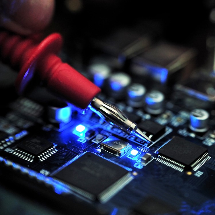
Many different test fixtures have been developed for functional testing of a PCBA (PCB assembly). Electrical connections may be made with connectors present on the PCBA or by test probes that contact test points defined by the PCB designer. Connectors on a test fixture are usually modified to allow for ease of mating and de-mating of the fixture’s connectors and the connectors on the PCBA to be tested. Connectors and the connectors on the PCBA to be tested. Connectors on the test fixture are also usually made easily replaceable, since they can wear out quickly with the multiple mating and de-mating cycles of production testing.
When making direct contact to test points on a PCBA, probes under the PCBA are typically fixed and the test fixture applies hold-down force to the top of the PCBA for reliable electrical connections to the test probes. If the PCBA being tested has test points on both sides of the board, then two probe plates are required, both of which must be precision aligned to each other and to the PCBA under test. With double-sided probing, the PCBA under test is typically fixed in place and the probes move in from both top and bottom when the fixture is operated.
Mengapa Memilih Bester

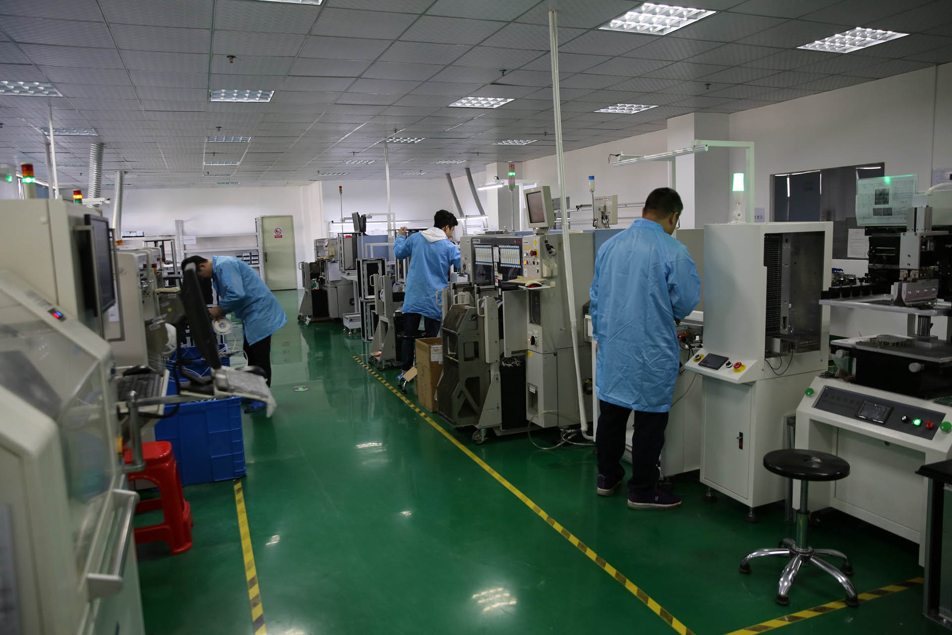
Kapasitas Perakitan yang Kuat
Dengan fasilitas canggih dan tim yang sangat terampil, kami memiliki kapasitas untuk menangani proyek perakitan PCB yang paling rumit sekalipun, memastikan produk Anda diproduksi secara efisien dan akurat.

Jaminan Kualitas
Proses kontrol kualitas kami yang ketat dan prosedur pengujian ekstensif menjamin bahwa setiap perakitan PCB yang kami produksi memenuhi standar industri tertinggi untuk keandalan dan kinerja, memberi Anda ketenangan pikiran dan kepercayaan diri dalam layanan kami.

Layanan Satu Atap
Dari fabrikasi dan desain PCB hingga sumber komponen dan pemrograman IC, Bester menawarkan berbagai layanan yang komprehensif di bawah satu atap, merampingkan proses produksi dan menghemat waktu dan tenaga Anda.

Perputaran Cepat
Komitmen kami terhadap waktu penyelesaian yang cepat berarti bahwa proyek perakitan PCB Anda akan selesai sesuai jadwal, sehingga Anda dapat memenuhi tenggat waktu produksi dan membawa produk Anda ke pasar dengan cepat.
Klien dan Sertifikasi

Industri yang Kami Layani

Otomotif
Kami memahami peran penting PCBA dalam industri otomotif. Dengan layanan PCBA kami yang komprehensif, kami memenuhi kebutuhan spesifik produsen otomotif, membantu mereka menghadirkan sistem elektronik yang andal dan berkinerja tinggi.
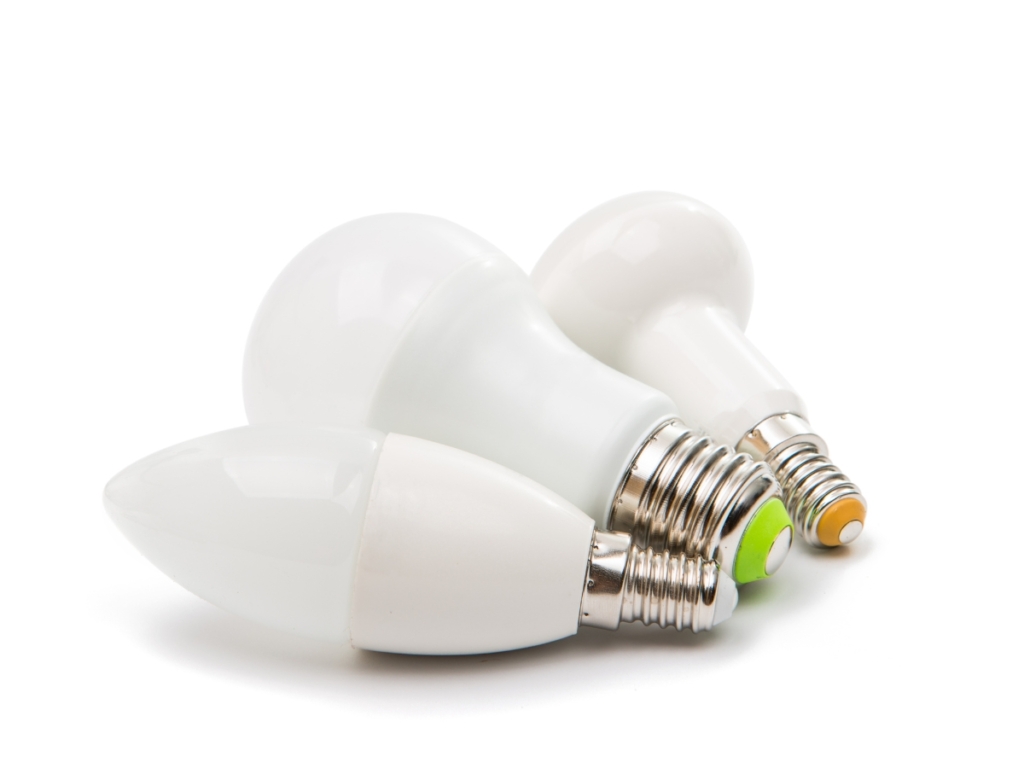
LED
Di pasar LED, Bester menyediakan solusi PCBA terbaik yang sangat penting untuk produksi produk pencahayaan LED berkualitas tinggi. Kami bekerja sama dengan produsen LED untuk memastikan bahwa PCBA mereka memenuhi persyaratan ketat efisiensi energi, daya tahan, dan kinerja.

Elektronik Konsumen
Bester melayani pasar elektronik konsumen dengan menawarkan berbagai layanan PCBA yang memungkinkan produksi perangkat elektronik yang inovatif dan ramah pengguna. Kami berkolaborasi dengan produsen elektronik konsumen untuk memastikan bahwa PCBA mereka memenuhi standar kualitas dan fungsionalitas tertinggi.

Industri
Di sektor industri, layanan PCBA Bester memainkan peran penting dalam pengembangan sistem elektronik yang andal dan efisien. Kami bekerja sama dengan produsen peralatan industri untuk memenuhi persyaratan khusus mereka, memastikan bahwa PCBA kami dapat bertahan dalam kondisi lingkungan yang keras dan memberikan kinerja yang optimal.
Kemampuan Manufaktur Elektronik di Bester
Kemampuan Manufaktur
- Kontrol Komponen ESD 100%
- 8 Jalur SMT
- 4 Garis DIP
- 40 Penyolderan Robot Otomatis
- Mesin CNC
- Pelapisan Konformal Otomatis
- Cetakan Injeksi
- Pencetakan 3D
Sertifikasi
- ISO 9001
- UL
- SGS
- IPC
- RoHS
- CE
- FCC
- SRDI (Perusahaan "Khusus, Penyempurnaan, Diferensial, Inovasi" Tiongkok)
- HNTE (Perusahaan Teknologi Tinggi dan Baru Tiongkok)
APLIKASI PCBA
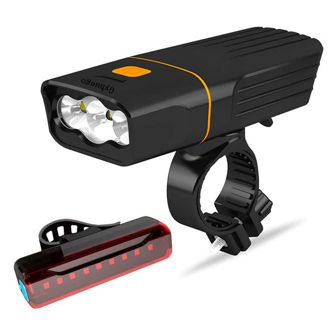
PCBA Lampu Sepeda
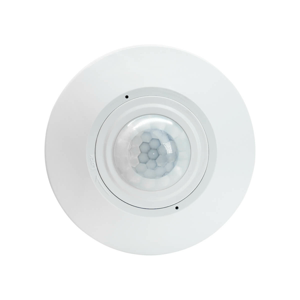
Sensor Gerak PIR PCBA
PCBA LED
PCB Assembly FAQs
Are you a certified PCB manufacturer?
Additive material process, also known as additive manufacturing, involves the123444412312312321on, such as a heated printhead or laser, to bind the layers together. Th an exact replica of the original 3D mg a fusing applicag a fusing applicaodel.
Are you a certified PCB manufacturer?
Additive material process, also known as additive manufacturing, involves the use of 3D printers to create a solid object from a 3D model. The process entails adding the material or filament layer by layer, and then using a fusing application, sug a fusing applicag a fusing applicag a fusing applicag a fusing applicag a fusing applicach as a heated printhead or laser, to bind the layers together. The end result is a 3D-printed object that is an exact replica of the original 3D model.
Are you a certified PCB manufacturer?
Additive material process, also known as additive manufacturing, involves the use of 3D printers to create a solid object from a 3D model. The process entails adding the material or filament layer by layer, and then using a fusing application, such as a heated printhead or laser, to bind the layers together. The end result is a 3D-printed object that is an exact replica of the original 3D model.
Do you offer quick turn PCBA service?
Additive material process, also known as additive manufacturing, involves the use of 3D printers to create a solid object from a 3D model. The process entails adding the material or filament layer by layer, and then using a fusing applicati
Do you accept small-batch orders?
Additive material process, also known as additive manufacturing, invg a fusing applicag a fusing applicag a fusing applicag a fusing applicag a fusing applicag a fusing applicag a fusing applicag a fusing applicaolves the use of 3D printers to create a solid object from a 3D model. The process entails adding the material or filament layer by layer, and then using a fusing application, such as a heated printhead or laser, to bind the layers together. The end result is a 3D-printed object that is an exact replica of the original 3D model.

Siap Memulai Proyek Perakitan PCB Anda?