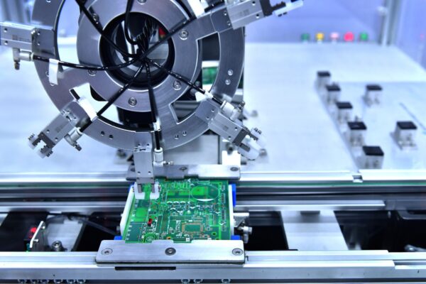
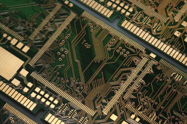
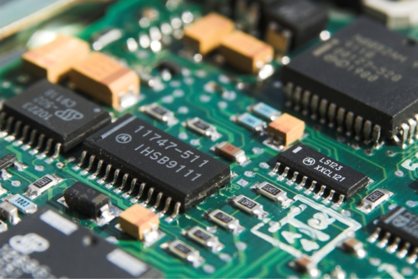
EMS PCBA is a critical aspect of the electronics industry, playing a vital role in the production of a wide range of electronic devices, from everyday consumer products to complex industrial and aerospace systems. This article provides a comprehensive overview of EMS PCBA, exploring its definition, manufacturing process, advanced technologies, testing methods, and failure analysis techniques. Whether you’re new to the world of electronics or an experienced researcher, this guide will provide you with valuable insights into this essential field.
What is EMS
EMS stands for Electronics Manufacturing Services. EMS companies are essentially the behind-the-scenes partners for companies that design and sell electronic products, known as original equipment manufacturers (OEMs). These EMS providers offer a wide range of services, including design, manufacturing, testing, and even supply chain management for electronic components and assemblies.
Think of it this way: an OEM might come up with the idea for a revolutionary new smartphone, but they might not have the facilities or expertise to actually build it. That’s where an EMS company steps in. They have the specialized equipment, skilled workforce, and industry knowledge to turn that smartphone concept into a reality.
EMS companies can range in size from small, specialized firms focusing on niche markets to large, global corporations with extensive capabilities.
Here are some of the key services offered by EMS providers:
- New Product Introduction (NPI): Helping OEMs bring new products to market quickly and efficiently.
- Printed Circuit Board Assembly (PCBA): The core service of assembling electronic components onto printed circuit boards.
- Box Build and System Integration: Assembling PCBAs into complete products or systems.
- Supply Chain Management: Sourcing and managing the components needed for manufacturing.
- Testing and Quality Assurance: Ensuring the quality and reliability of the products.
- Aftermarket Services: Providing repair, refurbishment, and other services after the product has been sold.
By partnering with EMS providers, OEMs can focus on their core competencies, such as product development and marketing, while leaving the complexities of manufacturing to the experts.
What is PCBA
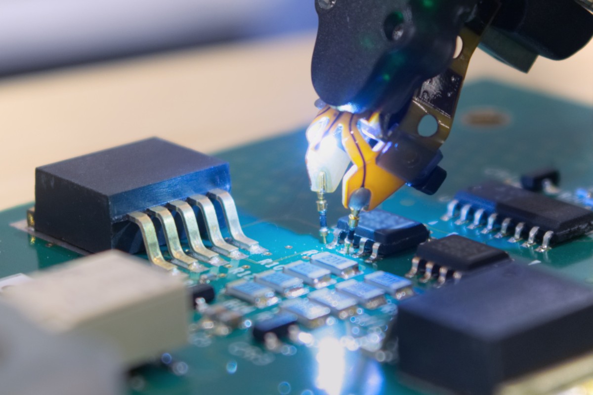
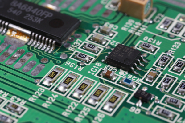
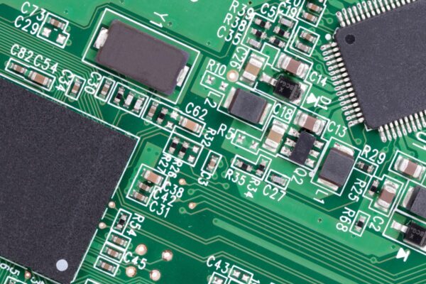
PCBA stands for Printed Circuit Board Assembly. In simple terms, a PCBA is the heart of most electronic devices. It’s a completed electronic assembly that consists of a printed circuit board (PCB) with all the necessary electronic components soldered onto it. The PCB acts as the foundation, providing both the mechanical support and the electrical pathways that allow the components to communicate and function together.
Imagine the PCB as the skeleton and nervous system of an electronic device. It provides the structure and the connections, while the components are like the organs, each performing a specific function. Together, they form the PCBA, which is responsible for the device’s overall functionality and connectivity.
Types of PCBAs
There are several different types of PCBAs, each with its own unique characteristics and applications:
- Rigid PCBs: These are the most common type of PCB, made from a solid, inflexible substrate material like FR-4 (a composite material made of woven fiberglass cloth with an epoxy resin binder). They are used in a vast array of applications, from simple devices like remote controls to complex systems like computer motherboards.
- Flexible PCBs: As the name suggests, these PCBs are made from a flexible substrate material, such as polyimide, that allows them to be bent or folded. This makes them ideal for applications where space is limited or where the PCB needs to conform to a curved surface. You’ll often find flexible PCBs in wearable devices like smartwatches, medical implants, and even in the intricate electronics of modern cars.
- Rigid-Flex PCBs: These PCBs combine the best of both worlds, featuring rigid sections for mounting components and flexible sections for making interconnections. This offers greater design flexibility and can reduce the need for connectors and cables, making the overall system more compact and reliable. Rigid-flex PCBs are often used in demanding applications like aerospace and medical devices, where both rigidity and flexibility are crucial.
- High-Frequency PCBs: These specialized PCBs are designed to operate at high frequencies, such as those used in radio frequency (RF) and microwave applications. They require specialized substrate materials and manufacturing processes to minimize signal loss and interference. High-frequency PCBs are essential for wireless communication, radar systems, and satellite communication.
- Aluminum-Backed PCBs: These PCBs use an aluminum substrate to provide excellent heat dissipation. They are particularly suitable for high-power applications where thermal management is critical, such as LED lighting, power supplies, and motor control circuits. The aluminum substrate helps to efficiently transfer heat away from heat-generating components, ensuring reliable operation.
What is EMS PCBA
EMS PCBA refers to the specialized services provided by Electronics Manufacturing Services (EMS) companies for the design, manufacturing, and testing of printed circuit board assemblies (PCBAs). Essentially, EMS providers offer a turnkey solution for PCBA, handling all aspects of the process from start to finish. This allows original equipment manufacturers (OEMs) to outsource their PCBA production and focus on other core aspects of their business, such as product development and marketing.
EMS PCBA is a specialized area within the broader field of electronics manufacturing services, requiring expertise in various areas, including circuit design, component selection, PCB layout, assembly processes, testing methodologies, and quality control.
Benefits of Using EMS PCBA Services
Why do companies choose to outsource their PCBA production to EMS providers? There are several compelling reasons:
- Cost Savings: EMS providers can often produce PCBAs at a lower cost than OEMs can achieve in-house. This is primarily due to economies of scale – EMS companies purchase large quantities of components and materials, allowing them to negotiate better prices. They also have highly optimized manufacturing processes that minimize waste and reduce labor costs.
- Quality Assurance: Reputable EMS providers have rigorous quality management systems in place, often certified to international standards like ISO 9001. This ensures that the PCBAs they produce meet the highest quality and reliability standards. They also have extensive testing capabilities to identify and eliminate any defects before the products reach the customer.
- Scalability: EMS providers offer flexibility in scaling production up or down to meet fluctuating demand. This is particularly important for OEMs that experience seasonal variations or are launching new products with uncertain market demand.
- Access to Expertise and Technology: EMS companies specialize in PCBA manufacturing and testing. They possess in-depth knowledge of the latest technologies, materials, and processes. They also invest heavily in state-of-the-art manufacturing equipment, which may be too expensive for individual OEMs to acquire.
- Faster Time to Market: By partnering with an EMS provider, OEMs can significantly reduce the time it takes to bring new products to market. EMS companies can streamline the PCBA manufacturing process and often provide design for manufacturability (DFM) support to optimize the PCBA design for efficient production.
Common Applications of EMS PCBA
EMS PCBA plays a crucial role in a wide range of industries, including:
- Consumer Electronics: This is perhaps the most visible application of EMS PCBA. From smartphones and tablets to laptops, televisions, gaming consoles, and smart home devices, EMS companies are responsible for manufacturing the PCBAs that power these everyday gadgets.
- Automotive: The automotive industry increasingly relies on sophisticated electronics for various functions, including engine control units (ECUs), infotainment systems, advanced driver-assistance systems (ADAS), and body electronics. EMS PCBA is essential for producing these complex and safety-critical automotive components.
- Medical Devices: The medical device industry has stringent quality and reliability requirements, making EMS PCBA a critical part of the manufacturing process. EMS companies produce PCBAs for a wide range of medical devices, including patient monitoring systems, diagnostic equipment, imaging systems, and even implantable devices.
- Industrial Equipment: Industrial equipment, such as programmable logic controllers (PLCs), motor drives, sensors, and robotics, relies heavily on robust and reliable PCBAs. EMS providers play a key role in manufacturing these components, ensuring they can withstand the harsh operating conditions often found in industrial environments.
- Aerospace and Defense: The aerospace and defense industries have extremely demanding requirements for their electronic systems. EMS PCBA is used to produce avionics, communication systems, radar systems, missile guidance systems, and other mission-critical components that must operate reliably in extreme conditions.
Key Components of a PCBA
A PCBA is made up of various components, each playing a specific role in the overall functionality of the assembly. These components can be broadly categorized into four main types:
Printed Circuit Board (PCB)
The PCB is the foundation of the PCBA, providing the necessary mechanical support and electrical connections for all the other components. It’s essentially a layered structure consisting of insulating material (such as FR-4, a composite material made of woven fiberglass cloth with an epoxy resin binder) with copper traces etched onto its surface. These copper traces form the conductive pathways that connect the various components, allowing electrical signals to flow between them.
PCBs can be single-sided (with copper traces on one side), double-sided (with copper traces on both sides), or multi-layered (with multiple layers of copper traces and insulating material stacked together). The complexity of the PCB depends on the complexity of the circuit it supports.
- Material Science Considerations: The choice of PCB substrate material is critical for the performance and reliability of the PCBA. Several factors need to be considered, including:
- Dielectric constant (Dk): This property affects the speed at which electrical signals propagate through the PCB and also influences the impedance of the traces.
- Loss tangent (Df): This property determines the amount of signal loss that occurs at high frequencies. Lower loss tangent values are desirable for high-frequency applications.
- Coefficient of thermal expansion (CTE): This property describes how much the PCB expands or contracts with changes in temperature. It’s crucial to match the CTE of the PCB material with the CTE of the components to prevent mechanical stress and potential failures.
- Glass transition temperature (Tg): This is the temperature at which the PCB substrate transitions from a rigid, glassy state to a softer, rubbery state. Higher Tg values are generally preferred for applications that involve high operating temperatures.
Active Components
Active components are the workhorses of the PCBA. They are capable of amplifying or switching electrical signals, enabling the circuit to perform complex functions. Some common examples of active components include:
- Integrated Circuits (ICs): These are miniature electronic circuits that contain a vast number of transistors, resistors, and other components fabricated on a single semiconductor chip. Examples include microprocessors, memory chips, analog-to-digital converters (ADCs), and digital-to-analog converters (DACs).
- Transistors: These are semiconductor devices that can amplify or switch electronic signals. There are two main types: bipolar junction transistors (BJTs) and field-effect transistors (FETs).
- Diodes: These are two-terminal semiconductor devices that allow current to flow in only one direction. Examples include rectifier diodes (used to convert AC to DC), Zener diodes (used for voltage regulation), and light-emitting diodes (LEDs).
Passive Components
Passive components, unlike active components, cannot amplify or switch electrical signals. However, they play essential roles in storing or dissipating energy within the circuit. Common examples include:
- Resistors: These components are used to limit the flow of current in a circuit.
- Capacitors: These components store electrical charge and are often used for filtering, timing, and energy storage.
- Inductors: These components store energy in a magnetic field and are commonly used in filters and oscillators.
Mechanical Components
Mechanical components provide mechanical support, connections, or other non-electrical functions within the PCBA. Examples include:
- Connectors: These components allow for the connection of external cables or devices to the PCBA.
- Switches: These components allow for the manual control of electrical circuits.
- Heat sinks: These components are designed to dissipate heat generated by active components, particularly power transistors and ICs. They help to prevent overheating and ensure the reliable operation of the PCBA.
PCBA Manufacturing Process
The PCBA manufacturing process is a complex and multi-stage process that involves several key steps, from initial design to final assembly and testing. Let’s explore each stage in detail:
Design and Engineering
The journey of a PCBA begins with the design and engineering phase. This is where the blueprint of the electronic circuit is created, components are selected, and the physical layout of the PCB is designed.
- Schematic Capture: The first step is to create a schematic diagram, which is a graphical representation of the electronic circuit. The schematic shows all the components that will be used in the circuit and how they are interconnected. Specialized electronic design automation (EDA) software is used for this purpose. Have you ever wondered how engineers translate a complex circuit idea into a visual representation? This is precisely what schematic capture does.
- Component Selection: Once the schematic is complete, the next step is to select the specific components that will be used on the PCBA. This involves considering various factors, such as the electrical characteristics of the components (e.g., voltage, current, power rating), their performance requirements, availability, and cost.
- PCB Layout: The PCB layout is the physical design of the printed circuit board. It determines the placement of the components on the board and the routing of the copper traces that connect them. This is a critical step that requires careful consideration of signal integrity, thermal management, and manufacturability.
- Design for Manufacturability (DFM): Throughout the design phase, engineers apply DFM principles to ensure that the PCBA can be manufactured efficiently and reliably. DFM involves optimizing the design to minimize manufacturing costs, reduce the risk of defects, and improve the overall quality of the PCBA.
Prototyping
Before moving to mass production, it’s essential to build and test a prototype of the PCBA. Prototyping allows engineers to verify the design, identify any potential issues, and make necessary adjustments before committing to large-scale production.
Prototyping typically involves producing a small number of PCBAs using the same processes that will be used for mass production. These prototypes are then subjected to rigorous testing to ensure they meet the required specifications and performance requirements.
Material Procurement
Once the design is finalized and the prototype is validated, the next step is to procure all the materials needed for PCBA manufacturing. This includes the PCB itself, the electronic components (active, passive, and mechanical), and other materials like solder paste and flux.
EMS providers typically have established relationships with a network of suppliers to ensure a reliable supply of high-quality materials.
- Supply Chain Management: Effective supply chain management is crucial for ensuring that the materials are available when needed and at the right price. This involves forecasting demand, managing inventory levels, and coordinating with suppliers to ensure timely delivery.
SMT Assembly
Surface Mount Technology (SMT) is the most widely used method for assembling PCBAs in modern electronics manufacturing. In SMT, components are mounted directly onto the surface of the PCB, rather than being inserted through holes as in traditional through-hole assembly.
Here are the key steps involved in the SMT assembly process:
- Solder Paste Printing: The first step is to apply solder paste to the PCB pads where the components will be mounted. This is typically done using a stencil, which is a thin sheet of metal with openings that correspond to the locations of the pads. A squeegee is used to push the solder paste through the stencil openings and onto the PCB.
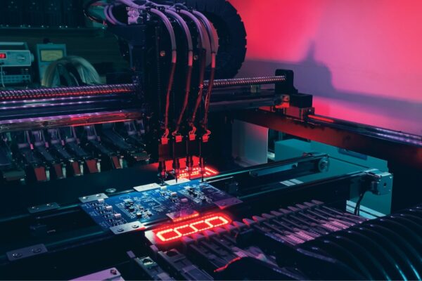
- Component Placement: Next, the components are placed onto the solder paste using a pick-and-place machine. These machines are highly automated and can place thousands of components per hour with high accuracy.
- Reflow Soldering: Once the components are placed, the PCBA is passed through a reflow oven. The oven heats the PCBA to a specific temperature profile, causing the solder paste to melt and then solidify, creating strong and reliable solder joints between the components and the PCB. Interplay of Design and Manufacturing: It’s important to note that the decisions made during the design phase, such as component placement and trace routing, have a direct impact on the SMT assembly process. For example, if components are placed too close together, it can be difficult to apply solder paste accurately and may lead to solder bridging (unintentional connections between adjacent pads). Similarly, poorly routed traces can affect the quality of the solder joints and the overall reliability of the PCBA.
Through-Hole Assembly
While SMT is the dominant assembly method, through-hole assembly is still used for certain types of components, particularly those that are larger or require a stronger mechanical connection to the PCB.
Here are the key steps involved in through-hole assembly:
- Component Insertion: Components with leads are inserted through pre-drilled holes in the PCB. This can be done manually or using automated insertion machines.
- Wave Soldering: After the components are inserted, the PCBA is passed over a wave of molten solder. The solder wave wets the leads of the components and the exposed pads on the underside of the PCB, creating solder joints.
Through-hole assembly is typically used for components like connectors, large capacitors, and transformers.
Inspection and Testing
After assembly, the PCBA undergoes rigorous inspection and testing to ensure that it meets the required quality standards and functions correctly.
- Inspection: Various inspection techniques are used to identify any defects in the PCBA, such as missing components, incorrect component placement, or solder joint problems. Common inspection methods include:
- Visual Inspection: This involves manually inspecting the PCBA using magnification aids to identify any visible defects.
- Automated Optical Inspection (AOI): AOI systems use cameras and image processing software to automatically inspect the PCBA for defects.
- X-ray Inspection: X-ray inspection is used to examine the internal structure of the PCBA and identify hidden defects, such as voids in solder joints or internal cracks in components.
- Testing: Electrical testing is performed to verify the functionality and performance of the PCBA. Common testing methods include:
- In-Circuit Testing (ICT): ICT uses a “bed of nails” fixture to make contact with test points on the PCB and verify the connections between components.
- Functional Testing (FCT): FCT involves applying power to the PCBA and simulating its normal operating conditions to verify that it functions as intended.
Conformal Coating and Potting
In some applications, the PCBA may need additional protection from environmental factors, such as moisture, dust, chemicals, or extreme temperatures. This is where conformal coating and potting come into play.
- Conformal Coating: Conformal coating involves applying a thin layer of protective material, such as acrylic, silicone, or urethane, to the surface of the PCBA. This coating conforms to the contours of the components and the PCB, providing a barrier against environmental contaminants.
- Potting: Potting is a more robust form of protection, where the entire PCBA is encapsulated in a protective material, typically a thermosetting resin. This provides a higher level of protection than conformal coating, but it also makes the PCBA more difficult to repair. Material Selection: The choice of conformal coating or potting material depends on the specific application and the environmental conditions that the PCBA will be exposed to. Factors to consider include the operating temperature range, the level of humidity, and the presence of any corrosive chemicals.
Final Assembly and Box Build
In many cases, the PCBA is just one part of a larger product or system. Final assembly, also known as box build or system integration, involves assembling the PCBA into its final enclosure or housing, along with other components such as power supplies, displays, cables, and mechanical parts.
This stage may involve connecting the PCBA to other sub-assemblies, installing software or firmware, and performing final testing to ensure that the complete product functions correctly.
Design for Manufacturability (DFM) Considerations
Design for Manufacturability (DFM) is a critical aspect of the PCBA design process. It involves optimizing the design to make it easier, faster, and more cost-effective to manufacture. Here are some key DFM considerations:
- Component Selection and Placement:
- Choose components that are readily available and suitable for automated assembly.
- Avoid placing components too close together, as this can make assembly and inspection difficult.
- Consider the thermal characteristics of components and their placement on the PCB to ensure proper heat dissipation. For example, high-power components should be placed away from heat-sensitive components and may require heat sinks or other cooling solutions.
- Trace Routing and Signal Integrity:
- Route traces carefully to minimize signal loss and interference, especially for high-speed signals.
- Use appropriate trace widths and spacing to maintain signal integrity. Wider traces have lower resistance and are less susceptible to signal degradation.
- Consider the use of impedance-controlled routing for high-frequency applications to ensure that the impedance of the traces matches the impedance of the components.
- Thermal Management:
- Design the PCB layout to facilitate heat dissipation from heat-generating components.
- Use thermal vias (small holes filled with conductive material) to transfer heat from one layer of the PCB to another.
- Consider the use of heat sinks, fans, or other cooling solutions for high-power components.
- Testability Considerations:
- Design the PCB layout to allow for easy access to test points during in-circuit testing (ICT).
- Consider the use of boundary scan testing, a technique that allows for testing of complex, high-density PCBAs without the need for physical test points.
Advanced PCBA Technologies
As electronic devices continue to become smaller, faster, and more complex, the demand for advanced PCBA technologies has grown significantly. These technologies push the boundaries of what’s possible in terms of miniaturization, performance, and functionality. Let’s explore some of the key advancements in PCBA technology:
High-Density Interconnect (HDI)
High-Density Interconnect (HDI) is a technology that enables the creation of smaller, lighter, and more complex PCBAs. HDI PCBs use finer lines and spaces, smaller vias (holes that connect different layers of the PCB), and higher connection pad densities compared to conventional PCBs.
- Microvias: One of the key features of HDI PCBs is the use of microvias. These are very small vias, typically less than 150 µm in diameter, that can be laser-drilled or photo-defined. Microvias allow for more efficient routing of traces and higher component density.
- Benefits of HDI:
- Reduced PCB size and weight: HDI allows for smaller and lighter PCBs, making it ideal for portable and wearable devices.
- Improved signal integrity: Shorter trace lengths due to higher density result in improved signal integrity and reduced signal loss.
- Higher component density: HDI enables the placement of more components in a smaller area, increasing the functionality of the PCBA.
- Challenges of HDI:
- Higher manufacturing costs: HDI PCBs are more expensive to manufacture than conventional PCBs due to the specialized equipment and processes required.
- More complex design and manufacturing processes: HDI design and manufacturing require specialized expertise and advanced software tools.
- Requires specialized equipment and expertise: Not all EMS providers have the capability to manufacture HDI PCBs.
System-in-Package (SiP)
System-in-Package (SiP) is a technology that integrates multiple integrated circuits (ICs) and other components into a single package. This approach can significantly reduce the size and complexity of the PCBA by combining multiple functions into a single component.
- Benefits of SiP:
- Reduced PCB size and weight: By integrating multiple components into a single package, SiP can significantly reduce the overall size and weight of the PCBA.
- Improved performance: Shorter interconnections between ICs within the SiP result in improved performance and reduced signal delays.
- Lower power consumption: SiP can help reduce power consumption by optimizing the interconnections between components.
- Challenges of SiP:
- Higher packaging costs: SiP packaging is typically more expensive than traditional single-chip packaging.
- More complex design and testing processes: Designing and testing SiPs can be more complex than designing and testing individual components.
- Thermal management: Thermal management can be challenging in SiPs due to the high component density within the package.
Embedded Components
Embedded components technology takes miniaturization a step further by embedding components within the layers of the PCB itself, rather than mounting them on the surface. This can further reduce the size and improve the performance of the PCBA.
- Benefits of Embedded Components:
- Reduced PCB size and weight: Embedding components within the PCB layers can significantly reduce the overall size and weight of the PCBA.
- Improved signal integrity: Shorter interconnections due to embedded components result in improved signal integrity and reduced signal loss.
- Reduced electromagnetic interference (EMI): Embedding components can help reduce EMI by shielding them within the PCB layers.
- Challenges of Embedded Components:
- Higher manufacturing costs: Manufacturing PCBs with embedded components is more expensive than traditional PCB manufacturing.
- More complex design and manufacturing processes: Designing and manufacturing PCBs with embedded components requires specialized expertise and advanced processes.
- Testing and rework: Testing and rework can be more difficult with embedded components, as they are not easily accessible once embedded within the PCB.
PCBA Testing and Quality Control
Testing and quality control are critical aspects of the PCBA manufacturing process. They ensure that the PCBA meets the required specifications, functions correctly, and is reliable over time. Various testing methods are employed throughout the manufacturing process, each with its own advantages and limitations.
In-Circuit Testing (ICT)
In-Circuit Testing (ICT) is a type of electrical testing that verifies the connections between components on the PCBA. It uses a “bed of nails” fixture, which is a platform with an array of spring-loaded pins that make contact with specific test points on the PCB.
- Test Procedure:
- The PCBA is placed on the bed of nails fixture, ensuring that the test points on the PCB align with the pins on the fixture.
- The ICT tester applies electrical signals to the test points and measures the responses.
- The tester compares the measured responses to the expected responses based on the circuit design. Any deviations indicate a potential defect, such as a short circuit, open circuit, or incorrect component value.
- Limitations of ICT:
- May not be able to detect all types of defects: ICT is primarily focused on detecting manufacturing defects related to component placement and soldering. It may not be able to detect functional failures or intermittent problems that only occur under specific operating conditions.
- Can be expensive to develop and maintain the test fixtures: The bed of nails fixtures are custom-designed for each PCBA, which can be costly and time-consuming.
- May not be suitable for all types of PCBAs: ICT may not be suitable for PCBAs with very high component density or those that use fine-pitch components, as it can be difficult to make reliable contact with the test points.
Functional Testing (FCT)
Functional Testing (FCT) is a type of electrical testing that verifies the overall functionality of the PCBA. Unlike ICT, which focuses on individual components and connections, FCT tests the PCBA as a complete system.
- Test Procedure:
- The PCBA is connected to a test system that simulates its normal operating environment. This may involve providing power to the PCBA and connecting it to other components or systems that it would interact with in the final product.
- The test system applies various inputs to the PCBA and monitors its outputs.
- The tester compares the measured outputs to the expected outputs based on the functional specifications of the PCBA. Any discrepancies indicate a functional failure.
- Limitations of FCT:
- May not be able to detect all types of defects: FCT is designed to verify the overall functionality of the PCBA, but it may not be able to detect certain types of defects, such as those that only occur under specific operating conditions or after prolonged use.
- Can be time-consuming and expensive to develop the test procedures: Developing comprehensive functional test procedures can be complex and require significant time and resources.
Automated Optical Inspection (AOI)
Automated Optical Inspection (AOI) is a type of visual inspection that uses cameras and image processing software to automatically inspect the PCBA for defects. AOI systems can detect a wide range of defects, such as missing components, incorrect component placement, solder bridges, and insufficient solder.
- Advantages of AOI:
- Fast and automated inspection process: AOI systems can inspect PCBAs much faster than manual visual inspection.
- Can detect a wide range of defects: AOI can detect many common manufacturing defects, improving overall product quality.
- Can be used for both pre-reflow and post-reflow inspection: AOI can be used to inspect PCBAs both before and after the reflow soldering process, allowing for early detection of defects.
- Limitations of AOI:
- May not be able to detect all types of defects: AOI relies on visual inspection, so it may not be able to detect defects that are hidden from view, such as internal cracks in components or voids in solder joints beneath components.
- Can be sensitive to lighting conditions and variations in component appearance: AOI systems can be affected by variations in lighting conditions and the appearance of components, which can lead to false positives (incorrectly identifying a good part as defective) or false negatives (failing to detect a real defect).
X-ray Inspection
X-ray inspection is a type of non-destructive testing that uses X-rays to create images of the internal structure of the PCBA. This allows for the detection of hidden defects that are not visible with other inspection methods, such as voids in solder joints, shorts between layers, and internal cracks in components.
- Advantages of X-ray Inspection:
- Can detect hidden defects: X-ray inspection is the only method that can reliably detect certain types of hidden defects, such as voids in BGA (Ball Grid Array) solder joints.
- Non-destructive: X-ray inspection does not damage the PCBA, so it can be used to inspect high-value or critical components.
- Limitations of X-ray Inspection:
- Can be expensive and time-consuming: X-ray inspection equipment is expensive, and the inspection process can be time-consuming, especially for complex PCBAs.
- Requires specialized equipment and trained operators: X-ray inspection requires specialized equipment and trained operators to interpret the X-ray images.
- May not be suitable for all types of PCBAs: X-ray inspection may not be effective for PCBAs with very thick or dense materials that absorb X-rays, making it difficult to obtain clear images.
- Novel Interpretations: X-ray inspection data can be used not only to identify defects but also to analyze the root causes of manufacturing problems. For example, by analyzing the size, shape, and distribution of voids in solder joints, engineers can gain insights into the reflow soldering process and identify areas for improvement.
Reliability Testing
Reliability testing is used to assess the long-term reliability of the PCBA under various operating conditions. It involves subjecting the PCBA to a series of stress tests that simulate the conditions it will experience during its expected lifespan.
- Types of Reliability Tests:
- Temperature Cycling: The PCBA is subjected to repeated cycles of high and low temperatures to simulate thermal stress. This helps to identify potential failures due to thermal expansion and contraction.
- Humidity Testing: The PCBA is exposed to high levels of humidity to simulate the effects of moisture. This helps to identify potential failures due to corrosion or moisture ingress.
- Vibration Testing: The PCBA is subjected to vibration to simulate the mechanical stresses it may experience during transportation or operation. This helps to identify potential failures due to mechanical fatigue or loose connections.
- Shock Testing: The PCBA is subjected to mechanical shocks to simulate sudden impacts. This helps to identify potential failures due to component breakage or solder joint failure.
Reliability testing can help to identify potential failure mechanisms and to estimate the lifespan of the PCBA under various operating conditions.
PCBA Failure Analysis Techniques
Failure analysis is the process of investigating PCBA failures to determine the root cause of the failure. It’s like detective work for electronics, where engineers use various tools and techniques to uncover why a PCBA failed and how to prevent similar failures in the future.
Failure analysis can help to improve the design, manufacturing, and testing processes, leading to more reliable and robust PCBAs.
Visual Inspection
Visual inspection is often the first step in failure analysis. It involves carefully examining the failed PCBA with the naked eye or using magnification aids, such as a microscope, to look for any obvious signs of damage or defects.
Visual inspection can often reveal obvious defects, such as:
- Burned or discolored components
- Cracked or broken components
- Cracked or lifted solder joints
- Physical damage to the PCB, such as cracks or delamination
Cross-Sectioning
Cross-sectioning is a destructive technique that involves cutting a section through the PCBA and polishing it to reveal the internal structure. This allows for a detailed examination of solder joints, vias (the holes that connect different layers of the PCB), and other internal features.
- Microstructural Analysis: Cross-sectioning allows for detailed examination of the microstructure of solder joints. This can reveal information about the quality of the soldering process, such as the presence of voids (air pockets), intermetallic compounds (brittle compounds that can form between the solder and the component leads or PCB pads), or other defects that can affect the long-term reliability of the solder joint.
Scanning Electron Microscopy (SEM)
Scanning Electron Microscopy (SEM) is a powerful technique that uses a focused beam of electrons to create highly magnified images of the surface of the PCBA. SEM can provide much higher resolution images than optical microscopy, revealing fine details that are not visible with the naked eye or a light microscope.
SEM can be used to examine:
- The morphology (shape and structure) of solder joints
- The surface of components to look for cracks, contamination, or other defects
- Fracture surfaces to determine the cause of a mechanical failure
Energy Dispersive X-ray Spectroscopy (EDS)
Energy Dispersive X-ray Spectroscopy (EDS) is an analytical technique that is often used in conjunction with SEM. It can determine the elemental composition of a specific area on the PCBA. When the electron beam from the SEM strikes the sample, it causes the atoms in the sample to emit characteristic X-rays. By analyzing the energy and intensity of these X-rays, EDS can identify the elements present and their relative concentrations.
EDS can be used to:
- Identify the composition of solder joints and check for the presence of intermetallic compounds or contaminants.
- Analyze the composition of component leads or pads to assess their solderability.
- Identify unknown materials or contaminants on the surface of the PCBA.
The Future of EMS PCBA
The field of EMS PCBA is constantly evolving, driven by advancements in technology, increasing demand for smaller and more powerful electronic devices, and the growing complexity of electronic systems. Here are some of the key trends that are shaping the future of EMS PCBA:
- Miniaturization: The trend toward smaller and more compact electronic devices will continue to drive the demand for advanced PCBA technologies, such as HDI, SiP, and embedded components. These technologies enable the creation of smaller, lighter, and more powerful PCBAs, which are essential for portable, wearable, and implantable devices.
- Increased Functionality: As electronic devices become more sophisticated, PCBAs will need to support a wider range of functions and higher levels of integration. This will require the use of more complex components, such as multi-core processors, high-capacity memory chips, and advanced sensors, as well as the development of new packaging and interconnect technologies.
- Higher Frequencies and Data Rates: The increasing demand for faster data transfer and wireless communication will drive the need for PCBAs that can operate at higher frequencies and support higher data rates. This will require the use of specialized materials with low dielectric loss and advanced signal integrity design techniques.
- Internet of Things (IoT): The growth of the Internet of Things (IoT) will create a massive demand for connected devices, many of which will require specialized PCBAs. These PCBAs will need to be small, low-power, and capable of wireless communication, posing new challenges for EMS providers.
- Artificial Intelligence (AI): AI is beginning to play a role in PCBA manufacturing, particularly in the areas of process optimization, quality control, and predictive maintenance. AI-powered systems can analyze large amounts of data from the manufacturing process to identify patterns, predict potential problems, and optimize production parameters.
- Automation and Robotics: Automation and robotics are playing an increasingly important role in PCBA manufacturing, improving efficiency, reducing costs, and enhancing quality. Robots are being used for tasks such as component placement, soldering, and inspection, while automated systems are being used to manage the flow of materials and track production data.
- Sustainability: Sustainability is becoming an increasingly important consideration in the electronics industry, and EMS providers are under pressure to reduce their environmental impact. This includes using more environmentally friendly materials, reducing energy consumption, and minimizing waste.
- Regionalization: There is a growing trend toward regionalization of EMS PCBA manufacturing, with companies seeking to establish manufacturing facilities closer to their customers or in regions with lower labor costs or favorable government incentives. This can help to reduce supply chain risks, improve responsiveness to customer needs, and reduce transportation costs.
These trends present both challenges and opportunities for EMS providers. To remain competitive, EMS companies will need to invest in new technologies, develop new capabilities, and adapt to the changing needs of their customers. They will also need to find ways to balance the increasing demand for miniaturization and functionality with the need for cost-effectiveness and sustainability.
The future of EMS PCBA will likely be characterized by:
- Increased collaboration: Closer collaboration between OEMs, EMS providers, and component suppliers will be essential to develop and manufacture increasingly complex PCBAs.
- Greater specialization: EMS providers may increasingly specialize in specific technologies or applications to differentiate themselves and meet the unique needs of their customers.
- Adoption of Industry 4.0 principles: The principles of Industry 4.0, such as connectivity, data analytics, and automation, will play an increasingly important role in PCBA manufacturing, enabling greater efficiency, flexibility, and responsiveness.
- Focus on talent development: As PCBA technology becomes more complex, EMS providers will need to invest in training and development to ensure they have the skilled workforce needed to design, manufacture, and test advanced PCBAs.
In conclusion, the field of EMS PCBA is undergoing a period of rapid transformation. The trends outlined above are driving significant changes in the way PCBAs are designed, manufactured, and tested. EMS providers that can adapt to these changes and embrace new technologies will be well-positioned to succeed in the years to come. The future of EMS PCBA promises to be an exciting one, filled with innovation and new possibilities.
