Die Oberflächenmontagetechnik (SMT) hat die Elektronikfertigung grundlegend verändert. Sie hat eine Ära der Miniaturisierung und der verbesserten Leistung bei der Montage von Leiterplatten (PCB) eingeleitet. Dieser Artikel befasst sich mit den Feinheiten der SMT, einschließlich ihrer Entwicklung, Vorteile und Auswirkungen auf verschiedene Branchen.
Was ist Oberflächenmontagetechnik?
SMT ist ein Verfahren zur Leiterplattenbestückung, bei dem die elektronischen Bauteile direkt auf die Oberfläche der Leiterplatte montiert werden. Im Gegensatz zur Durchstecktechnik müssen bei der SMT-Technik die Bauteile nicht durch gebohrte Löcher eingesetzt werden. Diese scheinbar einfache Änderung der Montagetechnik hat erhebliche Auswirkungen auf das Elektronikdesign und die Fertigung.
SMDs, oder oberflächenmontierte Bauteile, sind das Herzstück der SMT-Technik. Diese Bauteile wurden speziell für diese Montagemethode entwickelt und sind deutlich kleiner als ihre durchkontaktierten Gegenstücke. Sie verfügen oft über kurze Stifte, flache Kontakte oder sogar kleine Lötkugeln für den Anschluss. Zu den gängigen SMD-Bauteilen gehören Widerstände, Kondensatoren, Induktivitäten, Dioden, Transistoren und integrierte Schaltungen, die alle für eine effiziente Oberflächenmontage ausgelegt sind.
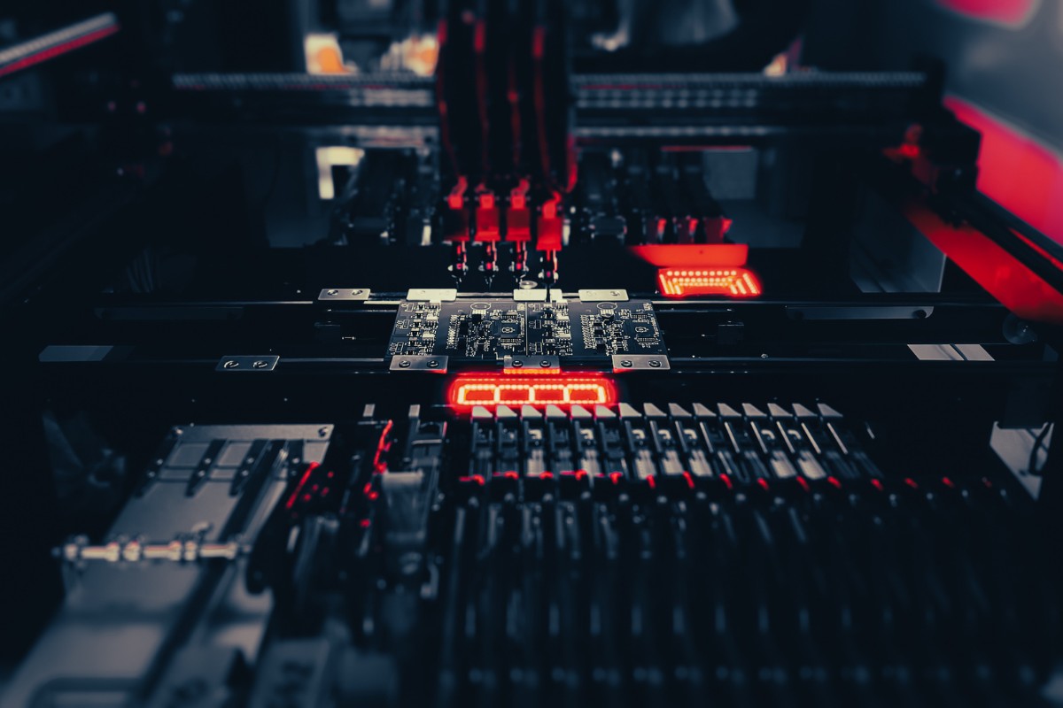
Der SMT-Bestückungsprozess ist präzise und automatisiert. Es beginnt mit dem Auftragen von Lotpaste auf die Leiterplatte mithilfe einer Schablone. Diese Paste, eine Mischung aus winzigen Lotpartikeln und Flussmittel, dient sowohl als Klebstoff als auch als leitendes Medium. Anschließend entnehmen Bestückungsautomaten die Bauteile von Spulen oder Tabletts und positionieren sie mit bemerkenswerter Genauigkeit auf der Leiterplatte, wobei oft Zehntausende von Bauteilen pro Stunde platziert werden.
Die Reflow-Lötphase ist die Phase, in der die Magie passiert. Die gesamte Platine, die nun mit Bauteilen bestückt ist, durchläuft einen Reflow-Ofen. Bei diesem kontrollierten Erhitzungsprozess schmilzt die Lötpaste und schafft dauerhafte elektrische und mechanische Verbindungen zwischen den Bauteilen und der Leiterplatte. Die Oberflächenspannung des geschmolzenen Lots hilft bei der Ausrichtung der Bauteile und korrigiert kleinere Platzierungsabweichungen.
Im Vergleich zur herkömmlichen Durchstecktechnik bietet diese Montagemethode zahlreiche Vorteile. Sie ermöglicht eine höhere Bauteildichte, kleinere Baugrößen und häufig eine bessere elektrische Leistung aufgrund kürzerer Verbindungswege. Die mit der SMT-Technik verbundene Automatisierung führt auch zu schnelleren Produktionszeiten und potenziell niedrigeren Herstellungskosten in großem Maßstab.
Die Entwicklung der Oberflächenmontagetechnik
Die Entwicklung von SMT von einem neuartigen Konzept zu einem Industriestandard zeigt das rasante Tempo der Innovation in der Elektronikfertigung. Ihre Wurzeln reichen bis in die 1960er Jahre zurück, als sie erstmals unter dem Namen "planare Montage" entwickelt wurde. Die SMT-Technik setzte sich jedoch erst in den 1980er Jahren in der Elektronikindustrie durch.
IBM spielte eine entscheidende Rolle bei der frühen Entwicklung und Einführung von SMT. Eine der ersten wichtigen Anwendungen war der Launch Vehicle Digital Computer, der in der Instrumenteneinheit für die Saturn IB und Saturn V Raketen der NASA eingesetzt wurde. Dieser frühe Erfolg zeigte das Potenzial von SMT für hochleistungsfähige, unternehmenskritische Anwendungen.
Der Übergang von der Durchstecktechnik zur SMT-Technologie erfolgte schrittweise, war aber einschneidend. Die Durchstecktechnik war jahrzehntelang der Standard, hatte aber ihre Grenzen bei der Größe der Leiterplatte, der Bauteildichte und der Fertigungseffizienz. Als die Elektronik immer komplexer wurde und die Nachfrage nach kleineren Geräten zunahm, erkannte die Industrie die Notwendigkeit eines neuen Ansatzes.
SMT hat diese Herausforderungen direkt angegangen. Durch die Montage von Bauteilen direkt auf der Oberfläche der Leiterplatte entfiel die Notwendigkeit, Löcher zu bohren, was Zeit und Kosten sparte. Vor allem aber ermöglichte sie eine deutlich höhere Bauteildichte und ebnete damit den Weg für den Miniaturisierungstrend, der die Unterhaltungselektronik seit Jahrzehnten bestimmt.
Die Einführung der SMT-Technik beschleunigte sich in den 1980er und 1990er Jahren. Bis 1986 machten oberflächenmontierte Bauteile etwa 10% des Marktes aus. Ein Jahrzehnt später dominierten sie die elektronischen High-Tech-Baugruppen. Diese rasche Verbreitung wurde durch mehrere Faktoren begünstigt, darunter die steigende Nachfrage nach tragbaren elektronischen Geräten, der Bedarf an leistungsfähigeren Computern und die Forderung nach effizienteren Herstellungsverfahren.
Der technologische Fortschritt im Bereich der SMT hat sich kontinuierlich weiterentwickelt. Die Bauteilgrößen sind drastisch geschrumpft, so dass einige moderne SMDs kaum noch sichtbar sind. Die Entwicklung von BGA-Gehäusen (Ball Grid Array), bei denen eine Reihe von Lötkugeln für die Anschlüsse verwendet wird, ermöglichte eine noch höhere Anschlussdichte und eine bessere Wärmeableitung.
Die Fertigungsanlagen haben sich parallel zur Bauteiltechnologie entwickelt. Moderne Bestückungsautomaten sind unglaublich schnell und präzise und können Zehntausende von Bauteilen pro Stunde mit einer Genauigkeit im Mikrometerbereich platzieren. Auch die Reflow-Öfen sind anspruchsvoller geworden und verfügen über mehrere Heizzonen und eine präzise Temperaturregelung, um den unterschiedlichen thermischen Anforderungen der verschiedenen Bauteile gerecht zu werden.
Verbesserungen in der Lötpasten- und Flussmitteltechnologie haben die Zuverlässigkeit von SMT-Verbindungen erhöht. Bleifreie Lote, die als Reaktion auf Umweltbedenken entwickelt wurden, sind bei vielen Anwendungen zum Standard geworden. Fortschritte in der Flussmittelchemie haben die Lötbarkeit verbessert und gleichzeitig die Notwendigkeit der Reinigung nach der Montage verringert.
Der Einfluss von SMT auf die Elektronikindustrie ist unbestreitbar. Sie hat die Entwicklung kleinerer, leichterer und leistungsfähigerer elektronischer Geräte ermöglicht, die wir heute als selbstverständlich betrachten. Smartphones, Tablets und tragbare Geräte verdanken ihre Existenz zu einem großen Teil den Fähigkeiten der SMT. Neben der Unterhaltungselektronik hat die SMT auch andere Branchen von der Automobilindustrie bis zur Luft- und Raumfahrt verändert und anspruchsvollere elektronische Systeme in Fahrzeugen, Flugzeugen und Satelliten ermöglicht.
Die Entwicklung von SMT ist noch lange nicht abgeschlossen. In dem Maße, wie wir die Grenzen der Miniaturisierung und Leistung von Elektronik immer weiter verschieben, entstehen auch neue Herausforderungen und Innovationen. Die Entwicklung von 3D-Packaging-Technologien und die Integration von SMT mit additiven Fertigungsverfahren sind nur einige Beispiele dafür, wie sich diese Technologie ständig anpasst und weiterentwickelt.
Vorteile der Oberflächenmontagetechnik
SMT bietet zahlreiche Vorteile, die es zur bevorzugten Methode für die Leiterplattenbestückung in den meisten modernen Elektronikanwendungen gemacht haben. Diese Vorteile erstrecken sich auf Design, Herstellung und Leistung.
Miniaturisierung und Platzersparnis
Durch SMT wird die Größe elektronischer Geräte drastisch reduziert. SMT-Komponenten sind von Natur aus kleiner als ihre durchkontaktierten Gegenstücke, oft um den Faktor zehn oder mehr. Diese Größenreduzierung ermöglicht eine wesentlich höhere Komponentendichte auf Leiterplatten.
SMT ermöglicht auch die Nutzung beider Seiten einer Leiterplatte für die Platzierung von Bauteilen. Durch die doppelseitige Bestückung verdoppelt sich der verfügbare Platz für Komponenten, was zu noch kompakteren Designs führt. Das Ergebnis sind kleinere, leichtere elektronische Geräte mit der gleichen oder einer größeren Funktionalität.
Diese Miniaturisierung war entscheidend für die Entwicklung der modernen tragbaren Elektronik. Smartphones beispielsweise vereinen eine Rechenleistung in einem Gerät im Taschenformat, für die noch vor wenigen Jahrzehnten ein Gerät in der Größe eines Schreibtisches erforderlich gewesen wäre. Wearable Technology, wie Smartwatches und Fitness-Tracker, wäre ohne die Raumeffizienz von SMT praktisch unmöglich.
Vorteile in der Fertigung
SMT bietet erhebliche Vorteile im Herstellungsprozess, was zu einer höheren Effizienz und potenziell niedrigeren Produktionskosten führt. Der Verzicht auf das Bohren von Löchern für Bauteilanschlüsse vereinfacht die Leiterplattenherstellung und reduziert den Materialabfall, spart Zeit und verringert das mit dem Bohren verbundene Fehlerrisiko.
Der Montageprozess selbst ist hoch automatisiert. Bestückungsautomaten können Bauteile schnell und präzise auf der Leiterplatte positionieren, wobei einige fortschrittliche Systeme in der Lage sind, über 100.000 Bauteile pro Stunde zu platzieren. Diese Geschwindigkeit und Präzision führen zu kürzeren Produktionszeiten und höherem Durchsatz im Vergleich zur Durchsteckmontage.
Das Reflow-Löten, die Methode zur Herstellung dauerhafter Verbindungen in SMT, ermöglicht das gleichzeitige Löten aller Komponenten auf einer Platine. Dies steht im Gegensatz zum sequenziellen Löten, das bei der Durchsteckmontage häufig erforderlich ist. Das Ergebnis ist ein gleichmäßigerer und zuverlässigerer Lötprozess mit geringerer thermischer Belastung der Leiterplatte und der Bauteile.
Vorteile in Bezug auf Leistung und Verlässlichkeit
SMT kann in mehreren Bereichen Leistungsvorteile bieten. Die kürzeren Leitungslängen und die geringeren parasitären Kapazitäten und Induktivitäten von SMT-Komponenten können zu einer besseren Hochfrequenzleistung führen. Dies ist besonders wichtig für Anwendungen wie drahtlose Kommunikation und digitale Hochgeschwindigkeitsschaltungen.
Richtig konstruierte SMT-Baugruppen können eine hervorragende mechanische Leistung aufweisen. Viele SMT-Bauteile sind stoß- und vibrationsfester als ihre durchkontaktierten Gegenstücke, was zum Teil auf ihre geringere Masse und das Fehlen von Leitungen zurückzuführen ist, die als Spannungskonzentratoren wirken können.
Die Planarität von SMT-Baugruppen kann auch zu einer verbesserten thermischen Leistung führen. Da die Bauteile in engem Kontakt mit der Leiterplattenoberfläche stehen, kann die Wärmeableitung effizienter sein, insbesondere in Kombination mit Techniken wie der Verwendung von Wärmeleitblechen oder Metallkernleiterplatten.
Designflexibilität und Innovation
SMT bietet Entwicklern eine noch nie dagewesene Flexibilität. Die Möglichkeit, Bauteile auf beiden Seiten der Leiterplatte zu platzieren, in Kombination mit der großen Vielfalt an verfügbaren SMT-Gehäusetypen, ermöglicht komplexere und innovativere Schaltungsdesigns.
Diese Flexibilität erstreckt sich auch auf die Arten von Leiterplatten, die verwendet werden können. SMT ist mit flexiblen und starr-flexiblen Leiterplatten kompatibel und eröffnet neue Möglichkeiten für Elektronik in unkonventionellen Formfaktoren. Dies war bei der Entwicklung von Produkten wie faltbaren Smartphones und tragbarer Elektronik von entscheidender Bedeutung.
Die geringe Größe von SMT-Komponenten ermöglicht eine effizientere Nutzung des Platzes auf der Leiterplatte für das Verlegen von Leiterbahnen. Dies kann zu einfacheren Platinenentwürfen mit weniger Lagen führen, was die Kosten senken und die Signalintegrität verbessern kann.
Kosten-Wirksamkeit
Die Anfangsinvestitionen in SMT-Anlagen können zwar beträchtlich sein, doch erweist sich die Technologie auf lange Sicht oft als kosteneffektiv, vor allem bei der Produktion hoher Stückzahlen. Durch die verstärkte Automatisierung sinken die Arbeitskosten und das Potenzial für menschliche Fehler. Die kleineren Bauteilgrößen und der geringere Materialverbrauch bei der Leiterplattenherstellung können ebenfalls zu Kosteneinsparungen beitragen.
Die höhere Zuverlässigkeit ordnungsgemäß entworfener und hergestellter SMT-Baugruppen kann zu einer Verringerung der Garantie- und Reparaturkosten während der Lebensdauer eines Produkts führen. Dies ist besonders wichtig in Branchen, in denen ein Geräteausfall erhebliche Folgen haben kann, z. B. in der Automobilindustrie oder in der Medizintechnik.
Die Kostenvorteile der SMT-Technik kommen vor allem bei der Großserienfertigung zum Tragen. Bei der Herstellung von Prototypen oder sehr geringen Stückzahlen können die anfänglichen Einrichtungskosten und die erforderliche Spezialausrüstung die Durchstecktechnik in einigen Fällen wirtschaftlicher machen.
Der Montageprozess für die Oberflächenmontage
Der SMT-Bestückungsprozess ist eine ausgeklügelte Abfolge von Schritten, von denen jeder für die Herstellung hochwertiger, zuverlässiger elektronischer Baugruppen entscheidend ist. Lassen Sie uns diesen Prozess im Detail erkunden, von der anfänglichen PCB-Vorbereitung bis zur abschließenden Qualitätskontrolle.
PCB-Vorbereitung
Der Prozess beginnt mit der Leiterplatte selbst. Das Leiterplattendesign für SMT erfordert eine sorgfältige Berücksichtigung von Pad-Layouts, Leiterbahnverlegung und der gesamten Leiterplattentopologie. Die Leiterplatte verfügt in der Regel über flache, metallische Pads - in der Regel mit Zinn, Blei, Silber oder Gold beschichtetes Kupfer -, die als Landeflächen für Komponenten dienen.
Ein entscheidendes Element ist das Auftragen der Lötmaske. Diese dünne, lackartige Polymerschicht wird auf die Leiterplatte aufgetragen, so dass nur die Lötpads freiliegen. Sie hilft, Lötbrücken zwischen eng beieinander liegenden Pads zu vermeiden und schützt die Kupferbahnen vor Oxidation.
Ein weiteres wichtiges Merkmal des SMT-Leiterplattendesigns ist die Aufnahme von Passermarken. Diese kleinen, in der Regel kreisförmigen Metallpads dienen als Referenzpunkte für die automatische Bestückungsanlage und gewährleisten eine präzise Ausrichtung der Komponenten.
Lötpaste Anwendung
Im nächsten Schritt wird Lotpaste auf die Leiterplatte aufgetragen. Lötpaste ist ein Gemisch aus winzigen Lötpartikeln (in der Regel mit einem Durchmesser von 20-45 Mikrometern), die in einem Flussmittel suspendiert sind. Diese Paste hält die Bauteile vorübergehend an ihrem Platz und bildet nach dem Schmelzen die dauerhaften Lötstellen.
Lötpaste wird in der Regel im Schablonendruckverfahren aufgetragen. Eine Metallschablone, die genau auf das Leiterplattendesign abgestimmt ist, wird auf die Platine gelegt. Die Lotpaste wird dann mit einem Rakel über die Schablone verteilt, wobei eine kontrollierte Menge der Paste auf jedes freiliegende Pad aufgebracht wird.
Das Volumen und die Konsistenz der Lötpaste sind entscheidend. Zu wenig Paste kann zu schwachen oder offenen Verbindungen führen, während zu viel zu Lötbrücken zwischen benachbarten Pads führen kann. Moderne Lotpastendruckmaschinen sind häufig mit geschlossenen Regelkreisen und Bildverarbeitungsinspektion ausgestattet, um einen gleichmäßigen, qualitativ hochwertigen Pastenauftrag zu gewährleisten.
Platzierung der Komponenten
Nach dem Auftragen der Lötpaste wird die Leiterplatte zur Bestückung mit Bauteilen weitergeleitet. Dies wird in der Regel von automatischen Bestückungsautomaten durchgeführt.
Diese Maschinen entnehmen Bauteile von Spulen, Tabletts oder Röhren und platzieren sie mit bemerkenswerter Genauigkeit auf der Leiterplatte. Moderne Systeme können Zehntausende von Bauteilen pro Stunde platzieren, wobei die Genauigkeit der Platzierung in Mikrometern gemessen wird.
Die Maschinen verwenden verschiedene Methoden, um eine genaue Platzierung zu gewährleisten. Optische Systeme erkennen Passermarken auf der Leiterplatte für die Gesamtausrichtung. Systeme zur Bauteilerkennung stellen sicher, dass jedes Teil vor der Platzierung korrekt ausgerichtet ist. Einige Systeme verwenden sogar Echtzeit-Röntgeninspektion für die kritischsten oder komplexesten Komponenten.
Die klebrige Beschaffenheit der Lötpaste trägt dazu bei, dass die Komponenten an ihrem Platz bleiben, sobald sie positioniert sind. Dies wird manchmal als die "grüne Stärke" der Baugruppe bezeichnet, da sie es ermöglicht, die Leiterplatte zur nächsten Stufe zu bewegen, ohne dass sich die Position der Komponenten verschiebt.
Reflow-Löten
Die bestückte Leiterplatte kommt dann in den Reflow-Ofen, wo die Lötpaste geschmolzen wird, um dauerhafte elektrische und mechanische Verbindungen herzustellen. Dieser Prozess ist komplexer als das einfache Erhitzen der Leiterplatte auf eine einzige Temperatur.
Ein typisches Reflow-Profil besteht aus mehreren unterschiedlichen Phasen:
- Vorheizen: Die Platine wird allmählich auf etwa 150 °C erwärmt, um eine gleichmäßige Erwärmung zu erreichen und das Flussmittel in der Lötpaste zu aktivieren.
- Thermisches Einweichen: Die Temperatur wird über einen bestimmten Zeitraum konstant gehalten, damit alle Komponenten eine einheitliche Temperatur erreichen. Dadurch wird der Temperaturschock minimiert und das Risiko von Defekten verringert.
- Reflow: Die Temperatur steigt schnell über den Schmelzpunkt des Lots (bei bleifreien Loten in der Regel um 220 °C). Das geschmolzene Lot bildet Verbindungen zwischen Bauteilanschlüssen und Leiterplattenpads.
- Abkühlung: Die Leiterplatte wird allmählich abgekühlt, damit das Lot erstarren und starke, zuverlässige Verbindungen bilden kann.
Das genaue Temperaturprofil wird sorgfältig auf der Grundlage von Faktoren wie Plattendicke, Bauteiltypen und Lotpastenzusammensetzung optimiert. Moderne Reflow-Öfen bieten mehrere unabhängig voneinander gesteuerte Heizzonen, um eine präzise Temperatursteuerung während des gesamten Prozesses zu erreichen.
Inspektion und Qualitätskontrolle
Nach dem Reflow-Prozess wird die bestückte Leiterplatte einer strengen Qualitätskontrolle unterzogen. Dies umfasst in der Regel eine Kombination aus automatisierten und manuellen Prüfverfahren.
Automatisierte optische Inspektionssysteme (AOI) verwenden hochauflösende Kameras und hochentwickelte Bildverarbeitungsalgorithmen, um Probleme wie fehlende Komponenten, falsche Ausrichtungen oder Lötfehler zu erkennen. Diese Systeme können Hunderte von Lötstellen pro Sekunde prüfen und liefern so schnelles Feedback zur Qualität der Baugruppe.
Für Bauteile mit verdeckten Lötstellen, wie z. B. Ball Grid Array (BGA)-Gehäuse, werden Röntgeninspektionssysteme eingesetzt. Diese können Probleme wie unzureichendes Lot, Hohlräume in Lötstellen oder Überbrückungen zwischen benachbarten Kugeln erkennen.
Auch die elektrische Prüfung ist entscheidend. Bei der In-Circuit-Prüfung (ICT) werden die Testpunkte auf der Leiterplatte mit einer Nagelbettvorrichtung kontaktiert, was eine schnelle elektrische Überprüfung der montierten Schaltungen ermöglicht. Funktionstests, bei denen die Leiterplatte unter Strom gesetzt und auf Herz und Nieren geprüft wird, dienen der abschließenden Überprüfung der ordnungsgemäßen Montage und des Betriebs.
Post-Montage-Prozesse
Je nach spezifischer Anwendung und Anforderungen können die bestückten Platten zusätzlichen Verfahren unterzogen werden. Diese können umfassen:
- Reinigung: Obwohl viele moderne SMT-Prozesse so konzipiert sind, dass sie nicht gereinigt werden müssen, kann es bei einigen Anwendungen, insbesondere in der Luft- und Raumfahrt oder im medizinischen Bereich, erforderlich sein, Flussmittelrückstände mit speziellen Reinigungslösungen und -geräten zu entfernen.
- Konforme Beschichtung: Auf Platinen, die für raue Umgebungen bestimmt sind, kann eine dünne Schutzschicht aufgetragen werden, um sie vor Feuchtigkeit, Staub und chemischen Verunreinigungen zu schützen und die langfristige Zuverlässigkeit der Baugruppe zu erhöhen.
- Underfill: Für bestimmte Anwendungen mit hoher Zuverlässigkeit kann ein flüssiges Epoxidharz unter BGAs oder andere große Komponenten geflossen werden. Diese Unterfüllung bietet nach dem Aushärten zusätzliche mechanische Unterstützung und Schutz gegen thermische Wechselbeanspruchungen.
Der SMT-Bestückungsprozess, von der ersten Vorbereitung der Leiterplatte bis zur abschließenden Prüfung, zeigt die Präzision und Raffinesse der modernen Elektronikfertigung. Jeder Schritt baut auf dem letzten auf und gipfelt in der Herstellung komplexer, zuverlässiger elektronischer Baugruppen, die unsere zunehmend vernetzte Welt versorgen.
Oberflächenmontage vs. Durchgangsbohrungstechnologie
Obwohl die SMT-Technik in vielen Anwendungen die vorherrschende Methode für die Leiterplattenbestückung geworden ist, spielt die Durchstecktechnik immer noch eine wichtige Rolle. Das Verständnis der Unterschiede zwischen diesen beiden Technologien ist für Ingenieure und Designer, die Entscheidungen über das Design und die Herstellung elektronischer Produkte treffen, von entscheidender Bedeutung.
Hauptunterschiede bei der Komponentenmontage
Der grundlegende Unterschied zwischen der SMT- und der Durchstecktechnik besteht darin, wie die Bauteile auf der Leiterplatte befestigt werden. Bei der SMT-Technik werden die Bauteile direkt auf die Oberfläche der Leiterplatte montiert. Ihre Anschlussdrähte berühren die Pads auf der Leiterplattenoberfläche. Bei durchkontaktierten Bauteilen hingegen werden die Anschlussdrähte durch in die Leiterplatte gebohrte Löcher geführt. Diese Leitungen werden dann auf der gegenüberliegenden Seite der Leiterplatte verlötet.
Dieser Unterschied in der Montagetechnik hat weitreichende Auswirkungen. SMT-Komponenten sind im Allgemeinen viel kleiner. Ein oberflächenmontierter Widerstand kann zum Beispiel weniger als einen Millimeter lang sein, während ein durchkontaktierter Widerstand mehrere Millimeter lang sein kann. Dieser Größenunterschied ist ein Schlüsselfaktor bei der Miniaturisierung von elektronischen Geräten.
Ein weiterer wesentlicher Unterschied besteht darin, dass SMT-Bauteile auf beiden Seiten einer Leiterplatte platziert werden können. Bauteile mit Durchgangsbohrungen werden aufgrund ihrer hervorstehenden Leitungen normalerweise nur auf einer Seite platziert. Diese doppelseitige Fähigkeit von SMT verdoppelt die verfügbare Fläche für Komponenten und ermöglicht komplexere Schaltungen auf einer gegebenen Leiterplattenfläche.
Vergleich der Herstellungsprozesse
Die Herstellungsverfahren für SMT- und Durchsteckmontage unterscheiden sich erheblich.
Vorbereitung der Leiterplatte: Die Durchsteckmontage erfordert das Bohren von Löchern in die Leiterplatte für jeden Bauteilanschluss. Dies erhöht den Zeit- und Kostenaufwand für die Herstellung der Leiterplatte und kann zu Defekten führen. Bei der SMT-Bestückung müssen lediglich Lötpunkte auf die Leiterplattenoberfläche gedruckt werden, was die Herstellung der Leiterplatte vereinfacht.
Platzierung von Bauteilen: Die Bestückung von Durchgangslöchern war traditionell ein manueller Prozess, obwohl es für einige Bauteiltypen automatische Bestückungsgeräte gibt. Die SMT-Bestückung ist sehr gut für die Automatisierung geeignet. Bestückungsautomaten können SMT-Bauteile schnell und genau positionieren, was die Montagegeschwindigkeit und -konsistenz erheblich erhöht.
Lötverfahren: Bei der Durchsteckmontage wird in der Regel das Wellenlöten verwendet, bei dem die bestückte Leiterplatte über eine Welle aus geschmolzenem Lot geführt wird. Dies kann schwierig zu kontrollieren sein, insbesondere bei Leiterplatten mit einer Mischung aus durchkontaktierten und oberflächenmontierten Komponenten. Beim SMT-Verfahren wird die Lötpaste vor der Bestückung auf die Leiterplatte aufgetragen und dann in einem sorgfältig kontrollierten Ofen geschmolzen. Dies ermöglicht eine präzisere Steuerung des Lötprozesses und kann zu konsistenteren, qualitativ hochwertigen Lötverbindungen führen.
Leistungs- und Zuverlässigkeitsaspekte
Sowohl mit der SMT- als auch mit der Durchstecktechnik lassen sich zuverlässige elektronische Baugruppen herstellen, aber jede hat ihre Stärken.
Elektrische Leistung: SMT bietet im Allgemeinen eine bessere Leistung bei Hochfrequenzanwendungen. Die kürzeren Leitungslängen und die geringeren parasitären Kapazitäten und Induktivitäten von SMT-Komponenten führen zu einer saubereren Signalübertragung und weniger elektromagnetischen Störungen. Dies macht SMT vorteilhaft für Anwendungen wie drahtlose Kommunikation oder digitale Hochgeschwindigkeitsschaltungen.
Mechanische Festigkeit: Komponenten mit Durchgangsbohrungen, deren Leitungen durch die Leiterplatte verlaufen, bieten oft stärkere mechanische Verbindungen. Dies kann bei Anwendungen, die starken Vibrationen oder mechanischen Belastungen ausgesetzt sind, wie z. B. in der Automobilindustrie oder in industriellen Umgebungen, von Vorteil sein. Gut konzipierte SMT-Baugruppen können auch eine ausgezeichnete mechanische Zuverlässigkeit aufweisen, und Techniken wie Underfill können ihre Robustheit weiter verbessern.
Thermische Leistung: Die thermischen Eigenschaften von SMT- und Durchgangsloch-Baugruppen können sich erheblich unterscheiden. Bauteile mit Durchgangsbohrungen, deren Leitungen durch die Leiterplatte verlaufen, können einen Pfad für die Wärmeableitung darstellen. SMT ermöglicht eine effizientere Nutzung von Kupferebenen zur Wärmeverteilung, und Techniken wie thermische Durchkontaktierungen können bei Bedarf zur Verbesserung der Wärmeableitung eingesetzt werden.
Designflexibilität und Komponentenverfügbarkeit
SMT bietet in vielerlei Hinsicht eine größere Designflexibilität. Die geringere Größe von SMT-Komponenten ermöglicht eine höhere Komponentendichte und eine komplexere Leiterbahnführung auf einer gegebenen Leiterplattenfläche. SMT ist auch besser mit flexiblen und starr-flexiblen Leiterplatten kompatibel und eröffnet Möglichkeiten für unkonventionelle Formfaktoren.
Die Durchstecktechnik bietet in bestimmten Bereichen immer noch Vorteile. Einige Spezial- oder Hochleistungskomponenten sind nur in Durchsteckgehäusen erhältlich. Die Durchstecktechnik wird auch oft für Bauteile bevorzugt, die ersetzt oder aufgerüstet werden müssen, wie Steckverbinder oder bestimmte Arten von Kondensatoren, da sie sich aufgrund der stärkeren mechanischen Verbindung besser für wiederholtes Einsetzen und Entfernen eignen.
SMT unterstützt eine breite Palette fortschrittlicher Gehäusetypen, wie BGAs und Quad Flat Packages (QFPs), die eine sehr hohe Anschlussdichte ermöglichen. Diese Gehäusetypen haben keine direkte Entsprechung in der Durchstecktechnik.
Kostenüberlegungen
Der Kostenvergleich zwischen SMT- und Durchstecktechnik hängt von verschiedenen Faktoren ab, darunter das Produktionsvolumen, die Auswahl der Bauteile und die spezifischen Anwendungsanforderungen.
Für die Großserienfertigung ist SMT im Allgemeinen kostengünstiger. Der höhere Automatisierungsgrad bei der SMT-Bestückung führt zu schnelleren Produktionszeiten und geringeren Arbeitskosten. Die geringere Größe der SMT-Bauteile kann auch zu einer kleineren Gesamtgröße der Leiterplatte führen, was die Materialkosten senkt.
Für die Produktion von Kleinserien oder Prototypen kann die Durchsteckmontage manchmal wirtschaftlicher sein. Die für die SMT-Bestückung erforderliche Ausrüstung stellt eine erhebliche Kapitalinvestition dar. Bei kleinen Produktionsserien können die Rüstkosten für die SMT-Bestückung die Effizienzgewinne aufwiegen.
Auch die Bauteilkosten können ein Faktor sein. Zwar sind viele Bauteile in SMT-Gehäusen aufgrund ihrer geringeren Größe und der hohen Produktionszahlen billiger, doch ist dies nicht immer der Fall. Einige spezialisierte Bauteile können teurer sein oder sind nur in Durchsteckgehäusen erhältlich.
Anwendungsspezifische Überlegungen
Die Entscheidung zwischen SMT und Durchsteckmontage hängt oft von der jeweiligen Anwendung ab.
Militär und Luft- und Raumfahrt: Diese Industriezweige bevorzugen häufig die Durchstecktechnik für kritische Komponenten, da sie unter extremen Bedingungen als zuverlässiger gilt. Die stärkere mechanische Verbindung von Komponenten mit Durchgangslöchern kann in Umgebungen mit hohen Vibrationen oder hohen G-Kräften von Vorteil sein.
Unterhaltungselektronik: SMT dominiert diesen Sektor aufgrund seiner Vorteile bei der Miniaturisierung und der Effizienz der Großserienproduktion. Die geringe Größe und das geringe Gewicht von SMT-Baugruppen sind entscheidend für tragbare Geräte wie Smartphones, Tablets und Wearables.
Kraftfahrzeuge: In modernen Fahrzeugen wird der größte Teil der Elektronik in SMT-Technik gefertigt, da kompakte, zuverlässige Steuermodule benötigt werden. Für bestimmte Anwendungen mit hohem Stromverbrauch oder hoher Zuverlässigkeit können weiterhin Bauteile mit Durchgangsbohrungen verwendet werden.
Industrielle Ausrüstung: In diesem Sektor wird häufig eine Mischung aus SMT- und Durchstecktechnik verwendet. SMT wird für Steuerelektronik bevorzugt, während Durchstecktechnik für robuste Hochleistungskomponenten oder Teile, die vor Ort ausgetauscht werden müssen, verwendet werden kann.
Viele moderne Leiterplattendesigns verwenden eine Kombination aus SMT- und Durchsteckkomponenten, wobei die Stärken der jeweiligen Technologie genutzt werden. Dieser hybride Ansatz ermöglicht es den Designern, Leistung, Zuverlässigkeit und Kosten auf der Grundlage der spezifischen Anforderungen jedes Teils der Schaltung zu optimieren.
Anwendungen und Auswirkungen von SMT auf die Industrie
Die SMT-Technologie hat zahlreiche Branchen tiefgreifend beeinflusst und das Produktdesign und die Fertigungsprozesse revolutioniert. Ihr Einfluss reicht von der Unterhaltungselektronik über die Luft- und Raumfahrt bis hin zu medizinischen Geräten und darüber hinaus. Sehen wir uns an, wie die SMT verschiedene Sektoren verändert hat.
Unterhaltungselektronik
Die Unterhaltungselektronikbranche hat sich durch die SMT-Technologie vielleicht am deutlichsten verändert. Diese Technologie hat den Trend zur Miniaturisierung, der die Unterhaltungselektronik in den letzten Jahrzehnten geprägt hat, entscheidend vorangetrieben.
Smartphones sind ein Paradebeispiel dafür. Diese Geräte vereinen Rechenleistung, drahtlose Kommunikationsmöglichkeiten, hochauflösende Displays und ausgeklügelte Kamerasysteme im Taschenformat. Ohne die hohe Bauteildichte und Miniaturisierung, die durch SMT ermöglicht werden, wären moderne Smartphones nicht möglich.
Auch Tablets und Laptops haben davon profitiert. Die Technologie hat dünnere, leichtere Geräte mit längerer Akkulaufzeit ermöglicht. Die Entwicklung von Laptops von sperrigen Geräten zu schlanken Ultrabooks ist weitgehend der Platzersparnis durch SMT zu verdanken.
Wearable Technology, wie Smartwatches und Fitness-Tracker, ist eine weitere Kategorie, die ihre Existenz der SMT verdankt. Diese Geräte erfordern extrem kompakte Schaltungsdesigns, damit sie in ihre kleinen Formfaktoren passen und dennoch fortschrittliche Funktionen wie Herzfrequenzüberwachung, GPS-Tracking und drahtlose Kommunikation bieten.
Im Bereich der Unterhaltungselektronik hat die SMT-Technik die Entwicklung immer ausgefeilterer und kompakterer Geräte ermöglicht. Moderne Smart-TVs verfügen über leistungsstarke Prozessoren und drahtlose Anschlussmöglichkeiten in schlanken Profilen. Spielkonsolen vereinen leistungsstarke Grafik- und Verarbeitungsfunktionen in relativ kleinen Gehäusen.
Kfz-Elektronik
Die Automobilindustrie hat sich mit der zunehmenden Integration von Elektronik stark gewandelt, und SMT hat dabei eine entscheidende Rolle gespielt.
Motorsteuergeräte (ECUs) sind immer ausgefeilter geworden und steuern alles von der Kraftstoffeinspritzung bis zur Emissionskontrolle mit zunehmender Präzision. Dank SMT können diese Geräte kompakt und dennoch leistungsstark sein und große Mengen an Sensordaten in Echtzeit verarbeiten.
Fortschrittliche Fahrerassistenzsysteme (ADAS) sind bei ihrer Implementierung stark auf SMT angewiesen. Funktionen wie adaptiver Tempomat, Spurhalteassistent und automatische Notbremsung erfordern kompakte, zuverlässige elektronische Steuermodule. Dank der geringen Größe von SMT-Baugruppen lassen sich diese Systeme nahtlos in Fahrzeuge integrieren.
Die Infotainmentsysteme in modernen Fahrzeugen sind immer fortschrittlicher geworden und bieten Funktionen wie Navigation, Smartphone-Integration und High-Fidelity-Audio. SMT ermöglicht es, diese komplexen Systeme auf dem begrenzten Platz im Armaturenbrett unterzubringen.
Die zunehmende Verbreitung von Elektro- und Hybridfahrzeugen hat neue Anforderungen an die Automobilelektronik geschaffen. Batteriemanagementsysteme, die für den sicheren und effizienten Betrieb dieser Fahrzeuge entscheidend sind, verlassen sich auf SMT für ihre kompakten, leistungsstarken Designs. Auch die Leistungselektronik für die Motorsteuerung in Elektrofahrzeugen profitiert von den hervorragenden thermischen und elektrischen Eigenschaften gut konzipierter SMT-Baugruppen.
Luft- und Raumfahrt und Verteidigung
Während die Luft- und Raumfahrt- sowie die Verteidigungsindustrie traditionell die Durchstecktechnik wegen ihrer vermeintlichen Zuverlässigkeitsvorteile bevorzugt haben, hat die SMT-Technik einen bedeutenden Aufschwung erlebt.
In der kommerziellen Luftfahrt hat die SMT-Technik die Entwicklung anspruchsvollerer Avioniksysteme ermöglicht. Flugmanagementcomputer, Navigationssysteme und Bordunterhaltungssysteme profitieren alle von der geringeren Größe und dem geringeren Gewicht von SMT-Baugruppen.
Auch die Satellitentechnik hat von SMT profitiert. Das geringere Gewicht von SMT-Baugruppen ist besonders wertvoll bei Satellitenanwendungen, wo jedes eingesparte Gramm an Bauteilgewicht zu erheblichen Kosteneinsparungen bei den Startkosten führen kann. SMT ermöglicht es auch, komplexere Funktionen in den begrenzten Raum zu packen, der in Satellitenkonstruktionen zur Verfügung steht.
Im militärischen Bereich werden SMT in tragbaren Kommunikationsgeräten eingesetzt, die kompaktere und leichtere Konstruktionen ermöglichen, die für den Einsatz im Feld entscheidend sind. Radarsysteme und Geräte für die elektronische Kriegsführung haben ebenfalls von den verbesserten Hochfrequenz-Leistungsmerkmalen von SMT profitiert.
Medizinische Geräte
Die Medizingeräteindustrie hat die SMT-Technik genutzt, um fortschrittlichere, kompaktere und patientenfreundlichere Geräte zu entwickeln.
Die tragbaren medizinischen Geräte haben sich erheblich weiterentwickelt. Geräte wie Blutzuckermessgeräte für Diabetiker sind kleiner und benutzerfreundlicher geworden. Wearable Health Tracker, die verschiedene Vitalparameter überwachen, sind aufgrund ihrer kompakten Bauweise auf SMT angewiesen.
Implantierbare medizinische Geräte stellen eine wichtige Anwendung der SMT dar. Herzschrittmacher und implantierbare Kardioverter-Defibrillatoren (ICDs) sind kleiner und ausgefeilter geworden, was den Patientenkomfort und die Langlebigkeit der Geräte verbessert. Cochlea-Implantate, die bei einigen Menschen mit schwerem Hörverlust das Gehör wiederherstellen, nutzen SMT, um komplexe Signalverarbeitungsfunktionen in einem kleinen implantierbaren Gerät unterzubringen.
Auch die diagnostische Ausrüstung hat sich stark verbessert. Ultraschallgeräte zum Beispiel haben sich von großen, auf einem Wagen basierenden Systemen zu tragbaren Geräten entwickelt, die leicht mitgeführt und am Ort der Behandlung verwendet werden können. Diese Miniaturisierung, die durch SMT ermöglicht wurde, hat die Zugänglichkeit fortschrittlicher medizinischer Bildgebung erweitert.
SMT hat auch die Entwicklung von anspruchsvolleren Laborgeräten ermöglicht. Automatisierte Blutanalysegeräte und DNA-Sequenzierungsmaschinen nutzen die hohe Komponentendichte von SMT, um komplexe analytische Fähigkeiten in relativ kompakte Formfaktoren zu packen.
Die Zuverlässigkeit von SMT-Baugruppen ist vor allem bei medizinischen Anwendungen von entscheidender Bedeutung, da ein Geräteausfall schwerwiegende Folgen haben kann. Strenge Qualitätskontrollverfahren und spezielle Konstruktionstechniken werden eingesetzt, um die langfristige Zuverlässigkeit von medizinischen Geräten mit SMT zu gewährleisten.
Industrie- und Telekommunikationsanlagen
Im Industriesektor hat SMT die Entwicklung kompakterer und ausgefeilterer Steuerungssysteme ermöglicht und damit zum Fortschritt der Automatisierung und der Industrie 4.0-Initiativen beigetragen.
Speicherprogrammierbare Steuerungen (SPS) sind dank der SMT-Technik leistungsfähiger und kompakter geworden. Dadurch konnten komplexere Steuerungssysteme in platzbeschränkten Industrieumgebungen implementiert werden.
SMT hat auch eine entscheidende Rolle bei der Entwicklung von Sensoren und Datenerfassungssystemen für industrielle Anwendungen gespielt. Das Internet der Dinge (IoT) stützt sich in hohem Maße auf kompakte, stromsparende Sensorknoten, die durch SMT ermöglicht werden.
In der Telekommunikationsbranche hat SMT maßgeblich zur Weiterentwicklung der Netzinfrastruktur beigetragen. Router, Switches und Mobilfunk-Basisstationen sind kompakter und energieeffizienter geworden und bieten gleichzeitig mehr Möglichkeiten zur Datenverarbeitung.
Die Entwicklung der 5G-Technologie mit ihren Anforderungen an Hochfrequenzbetrieb und kompakte Geräte ist besonders von der SMT abhängig. Die Fähigkeit, dichte, leistungsstarke HF-Schaltungen zu erstellen, ist entscheidend für die Implementierung der fortschrittlichen Antennenanordnungen und der für 5G-Netze erforderlichen Signalverarbeitung.
Auswirkungen auf Produktion und Lieferkette
Über ihre direkten Anwendungen hinaus hat die SMT einen tiefgreifenden Einfluss auf die Herstellungsprozesse in der Elektronik und die globalen Lieferketten.
Der hohe Automatisierungsgrad in der SMT-Bestückung hat zu erheblichen Veränderungen bei den Anforderungen an die Arbeitskräfte in der Fertigung geführt. Während der Bedarf an manuellen Montagearbeitern gesunken ist, ist gleichzeitig der Bedarf an qualifizierten Technikern für die Bedienung und Wartung der hochentwickelten SMT-Anlagen gestiegen.
SMT hat auch die Art und Weise beeinflusst, wie elektronische Produkte entworfen und Prototypen hergestellt werden. Die Verfügbarkeit von SMT-Bauteilen und -Bestückungsdienstleistungen hat es Start-ups und kleinen Unternehmen erleichtert, elektronische Produkte zu entwickeln und herzustellen, was zur Innovation im Technologiesektor beigetragen hat.
Die globale Elektronik-Lieferkette wurde durch die SMT-Technologie geprägt. Die Technologie hat die Konzentration der Massenfertigung von Elektronikprodukten in Regionen mit niedrigeren Arbeitskosten ermöglicht, da der automatisierte Charakter der SMT-Bestückung die Auswirkungen der Lohnkostenunterschiede verringert.
Die Zulieferer von Bauelementen haben ihr Produktangebot an die Anforderungen der SMT angepasst. Die Entwicklung von immer kleineren Bauteilgehäusen und die Umstellung auf bleifreie Lote sind direkte Ergebnisse der weit verbreiteten Einführung von SMT.
Der Bedarf an spezialisierten SMT-Anlagen hat neue Märkte für Anbieter von Fertigungstechnologie geschaffen. Unternehmen, die sich auf Bestückungsautomaten, Reflow-Öfen und Inspektionssysteme spezialisiert haben, sind zu wichtigen Akteuren im Ökosystem der Elektronikfertigung geworden.
SMT hat auch die Fortschritte in der Leiterplattenherstellungstechnologie vorangetrieben. Das feine Raster und die hohe Dichte der SMT-Komponenten haben die Leiterplattenhersteller dazu veranlasst, Möglichkeiten zur Herstellung von Leiterplatten mit feineren Leiterbahnen, kleineren Durchgangslöchern und mehr Schichten zu entwickeln.