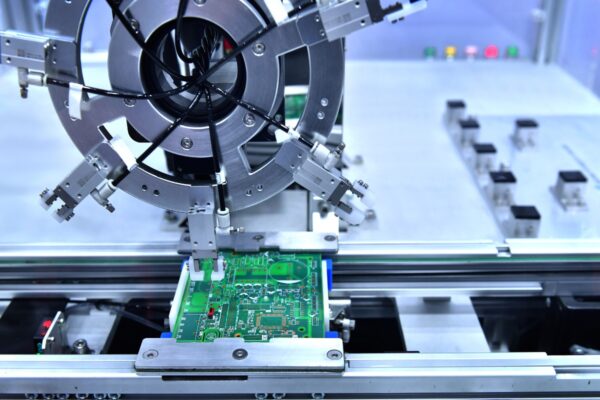
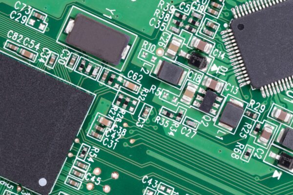
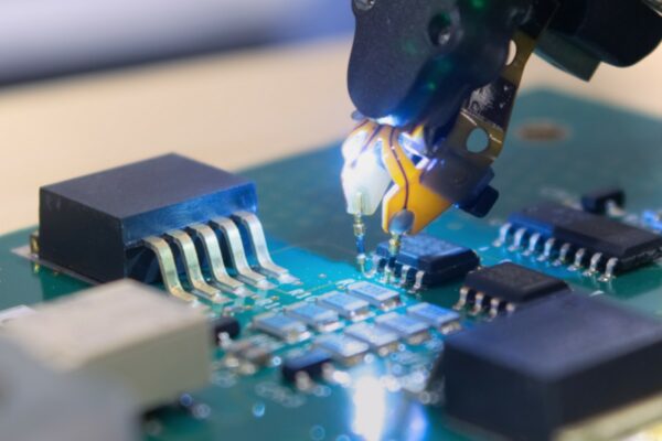
The world of electronics manufacturing is replete with acronyms, often used interchangeably, leading to a haze of confusion even amongst seasoned professionals. Two such terms, Circuit Card Assembly (CCA) and Printed Circuit Board Assembly (PCBA), are frequently at the heart of this ambiguity. While seemingly similar, a closer examination reveals subtle yet significant distinctions that impact design, manufacturing, and testing processes.
Defining the Core: Unpacking the Printed Circuit Board (PCB)
Before we delve into the intricacies of CCA and PCBA, it’s imperative to establish a solid understanding of the fundamental building block: the Printed Circuit Board (PCB). Often referred to as the “canvas” of electronics, the PCB provides the mechanical support and electrical connections for electronic components.
PCB Composition and Fabrication: A Layered Approach
A PCB is far more than just a green board. It’s a meticulously engineered composite structure, typically consisting of multiple layers of different materials. The most common substrate material is FR-4, a glass-reinforced epoxy laminate, chosen for its balance of cost, durability, and electrical insulation properties. However, specialized applications might demand alternatives like CEM (Composite Epoxy Material), PTFE (Polytetrafluoroethylene, commonly known as Teflon) for high-frequency circuits, or even flexible polyimide for flexible circuits.
Each PCB layer serves a specific purpose. Copper layers, etched with intricate patterns, form the conductive pathways that interconnect components. The fabrication process is a complex sequence of steps, including:
- Imaging: Transferring the circuit design onto the copper layers using photolithography.
- Etching: Chemically removing unwanted copper to create the desired circuit traces.
- Drilling: Creating holes (vias) for connecting different layers and mounting through-hole components.
- Plating: Depositing copper in the drilled holes to establish inter-layer connections.
- Lamination: Bonding multiple layers together under heat and pressure to form a single, cohesive structure.
- Solder Mask Application: Applying a protective layer (often green) to prevent solder bridges and protect the copper traces.
- Silkscreen Printing: Adding labels and markings for component identification and assembly guidance.
The precision and quality of these fabrication steps are paramount to the overall performance and reliability of the final product.
PCB Design Considerations: From Schematic to Layout
The journey from a conceptual circuit to a physical PCB begins with schematic capture. This involves translating a circuit diagram, which represents the functional relationships between components, into a schematic, a detailed representation of the circuit’s connectivity.
Component placement is a critical aspect of PCB layout. Optimal placement minimizes signal path lengths, reduces electromagnetic interference (EMI), and facilitates efficient thermal management. For instance, sensitive analog components should be placed far from noisy digital components to prevent signal degradation.
Routing, the process of connecting components with copper traces, is another crucial step. Careful routing is essential for maintaining signal integrity, especially in high-speed circuits. Factors like impedance control, crosstalk minimization, and trace width optimization must be meticulously considered.
Design rules and constraints, often enforced by PCB design software, play a vital role in ensuring manufacturability. These rules define parameters like minimum trace width, spacing between traces, and hole sizes, ensuring that the PCB can be reliably fabricated.
PCB Types and Their Applications: A Spectrum of Functionality
PCBs come in various forms, each tailored to specific application requirements.
- Single-sided PCBs: The simplest type, with circuitry on only one side of the substrate. They are cost-effective but limited in complexity.
- Double-sided PCBs: Featuring circuitry on both sides, offering increased component density and routing flexibility.
- Multilayer PCBs: Composed of multiple layers of circuitry, enabling complex designs and high component density. They are commonly used in sophisticated electronic devices like computers and smartphones.
- Rigid PCBs: The most common type, using rigid substrate materials like FR-4.
- Flex PCBs: Constructed with flexible substrates like polyimide, allowing them to bend and conform to specific shapes. They are ideal for applications requiring flexibility, such as wearable devices and medical implants.
- Rigid-flex PCBs: Combining the benefits of both rigid and flex PCBs, offering both structural stability and flexibility. They are often used in applications with space constraints and complex geometries.
- High-Density Interconnect (HDI) PCBs: Characterized by finer features, smaller vias, and higher wiring density. They enable miniaturization and are essential for high-performance devices.
- Specialized PCBs: Designed for specific applications, such as RF/microwave circuits, power electronics, and high-temperature environments.
The choice of PCB type depends on factors like circuit complexity, operating environment, mechanical constraints, and cost considerations.
Circuit Card Assembly (CCA): The Populated PCB
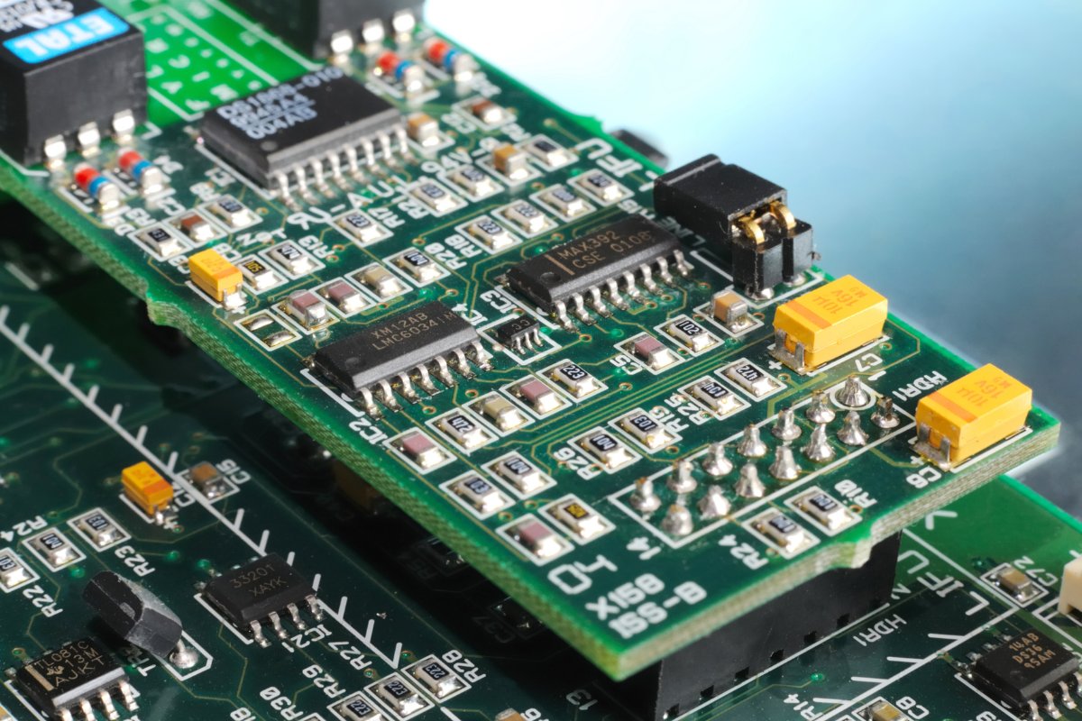
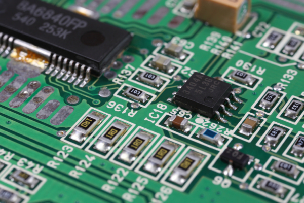
With the PCB foundation laid, we can now turn our attention to Circuit Card Assembly. In essence, CCA refers to the process of populating a bare PCB with electronic components, transforming it into a functional electronic circuit. It’s the stage where the carefully designed PCB comes to life.
Component Selection and Procurement: Balancing Performance and Reliability
The performance and reliability of a CCA hinge on the careful selection and procurement of electronic components. This involves choosing the right mix of active components (e.g., transistors, integrated circuits) and passive components (e.g., resistors, capacitors, inductors).
Component packaging plays a crucial role. Surface Mount Devices (SMDs) like SOIC, QFP, and BGA are designed for Surface Mount Technology (SMT), while through-hole components like DIP and axial/radial leaded devices are used in Through-Hole Technology (THT). The choice of package type impacts the assembly process, component density, and overall size of the CCA.
Selection criteria extend beyond basic functionality. Factors like operating temperature range, voltage and current ratings, tolerance, frequency response, and long-term reliability must be meticulously evaluated. The availability and lead time of components are also critical, especially in today’s complex global supply chains. Furthermore, the growing concern over counterfeit components necessitates robust verification and authentication processes.
Assembly Processes: SMT, Through-Hole, and Mixed Technologies
The two primary methods for assembling components onto a PCB are Surface Mount Technology (SMT) and Through-Hole Technology (THT).
Surface Mount Technology (SMT)
The dominant assembly method today, SMT involves mounting components directly onto the surface of the PCB. The process typically includes:
- Solder Paste Application: Applying solder paste, a mixture of solder powder and flux, to the component pads on the PCB using a stencil.
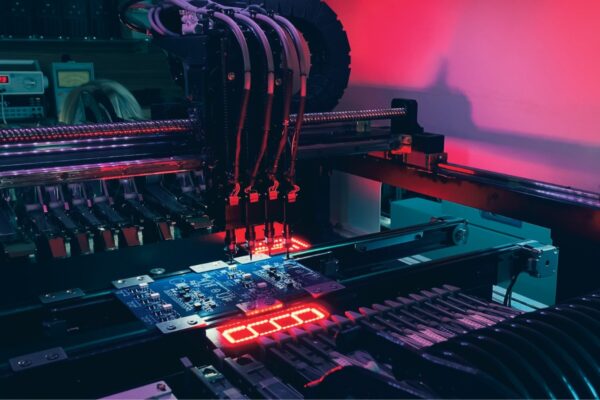
- Component Placement: Precisely placing SMDs onto the solder paste using automated pick-and-place machines.
- Reflow Soldering: Heating the entire assembly in a reflow oven to melt the solder paste, creating electrical and mechanical connections between the components and the PCB.
Through-Hole Technology (THT)
In THT, component leads are inserted through pre-drilled holes in the PCB and soldered on the opposite side. The process typically involves:
- Component Insertion: Manually or automatically inserting component leads through the holes.
- Wave Soldering: Passing the underside of the PCB over a wave of molten solder, soldering all the through-hole connections simultaneously.
- Selective Soldering: Using a localized solder fountain or a robotic soldering arm to solder specific through-hole components, often used in mixed technology assemblies.
Mixed Technology Assembly
Many modern electronic devices utilize a combination of SMT and THT, leveraging the advantages of both technologies. This approach requires careful planning and execution to ensure compatibility between the different assembly processes.
Advanced assembly techniques like Package on Package (PoP), where multiple components are stacked vertically, and flip-chip, where the die is directly attached to the PCB, are also employed for specialized applications requiring high density and performance.
Testing and Inspection: Ensuring Functionality and Conformance
Testing and inspection are crucial steps in the CCA process, ensuring that the assembled board functions correctly and meets the required quality standards.
- In-Circuit Test (ICT): Often referred to as “bed of nails” testing, ICT involves using a fixture with spring-loaded probes to contact test points on the CCA, verifying component values, checking for shorts and opens, and ensuring proper component placement.
- Functional Test (FCT): FCT verifies the overall functionality of the CCA by simulating its operating environment and applying inputs and measuring outputs. It ensures that the assembled board performs as intended.
- Automated Optical Inspection (AOI): AOI systems use cameras and image processing algorithms to inspect the CCA for defects like missing components, incorrect component orientation, solder bridges, and insufficient solder.
- X-ray Inspection: X-ray inspection is used to examine hidden solder joints, particularly for BGA components, where the solder connections are underneath the package. It can also detect internal defects within components.
These testing and inspection methods, often used in combination, provide a comprehensive assessment of the CCA’s quality and functionality.
CCA Standards and Certifications: Navigating the Regulatory Landscape
The electronics assembly industry is governed by various standards and certifications that ensure quality, reliability, and safety.
- IPC Standards: IPC, a global trade association, publishes widely recognized standards for electronics assembly. IPC-A-610, “Acceptability of Electronic Assemblies,” defines acceptance criteria for CCAs, covering aspects like component placement, soldering quality, and cleanliness. J-STD-001, “Requirements for Soldered Electrical and Electronic Assemblies,” specifies process control requirements for soldering.
- ISO Certifications: ISO 9001, a general quality management system standard, is commonly adopted by electronics assembly companies. ISO 13485, specifically for medical devices, sets more stringent requirements for quality and risk management.
- Industry-Specific Standards: Certain industries have their own specific standards. For example, the aerospace industry uses MIL-STD specifications, while the automotive industry relies on standards like IATF 16949.
- RoHS and REACH Compliance: Environmental regulations like RoHS (Restriction of Hazardous Substances) and REACH (Registration, Evaluation, Authorisation and Restriction of Chemicals) restrict the use of certain hazardous materials in electronic products, impacting component selection and manufacturing processes.
Printed Circuit Board Assembly (PCBA): A Holistic Perspective
While CCA focuses on the populated board, Printed Circuit Board Assembly encompasses a broader scope, encompassing the entire process from design to the final assembled product, ready for integration into a larger system. It’s a more holistic view of electronics assembly.
PCBA as a Superset: Encompassing CCA and Beyond
PCBA can be considered a superset of CCA. It includes not only the population of the PCB with components (the CCA process) but also additional steps like:
- Enclosure Assembly: Integrating the CCA into a housing or enclosure.
- Cable and Wire Harness Assembly: Connecting the CCA to other parts of the system using cables and wire harnesses.
- Conformal Coating or Potting: Applying a protective coating to the CCA to enhance its resistance to environmental factors like moisture, dust, and chemicals.
- Box Build: Assembling the complete product, including the CCA, enclosure, power supply, and other components.
- System-Level Testing: Testing the fully assembled product to ensure it functions correctly as a complete system.
PCBA, therefore, represents a more comprehensive approach to electronics assembly, considering the final product and its intended application.
Design for Manufacturability (DFM) and Design for Assembly (DFA)
Design for Manufacturability (DFM) and Design for Assembly (DFA) are crucial considerations in PCBA. DFM focuses on optimizing the PCB design for efficient and cost-effective manufacturing. This includes considerations like:
- Panel Design: Optimizing the layout of multiple PCBs on a single panel to minimize material waste and reduce fabrication costs.
- Component Selection: Choosing components that are readily available and compatible with automated assembly processes.
- Test Point Placement: Strategically placing test points to facilitate in-circuit testing.
DFA, on the other hand, focuses on simplifying the assembly process, reducing assembly time and cost. This involves:
- Component Orientation: Standardizing component orientation to facilitate automated placement.
- Minimizing Component Variety: Reducing the number of different component types to simplify the assembly process and reduce inventory costs.
- Using Standard Fasteners: Employing standard screws and other fasteners to streamline assembly.
Early collaboration between design and manufacturing engineers is essential to ensure that DFM and DFA principles are effectively implemented.
Supply Chain Management: From Component Sourcing to Final Product
Effective supply chain management is critical for successful PCBA. This involves managing the flow of materials, information, and finances from component suppliers to the end customer.
- Component Sourcing Strategies: Developing robust sourcing strategies to ensure a reliable supply of components, considering factors like cost, quality, lead time, and supplier reliability. This may involve diversifying suppliers, building strategic partnerships, and implementing risk mitigation measures.
- Inventory Management: Implementing efficient inventory control systems to minimize inventory holding costs while ensuring that components are available when needed. This often involves using techniques like Just-In-Time (JIT) inventory management.
- Logistics and Shipping: Managing the transportation and delivery of materials and finished products, ensuring timely delivery and minimizing transportation costs.
- Risk Management: Identifying and mitigating potential supply chain risks, such as component shortages, natural disasters, and geopolitical instability. This may involve developing contingency plans and building resilience into the supply chain.
Quality Assurance and Reliability Engineering in PCBA
Quality assurance and reliability engineering are integral to PCBA, ensuring that the final product meets the required quality standards and performs reliably over its intended lifespan.
Quality Management Systems (QMS)
Implementing a robust QMS, often based on ISO 9001, to ensure consistent quality throughout the PCBA process. This involves establishing procedures, documenting processes, and conducting regular audits.
Reliability Testing
Conducting various reliability tests to assess the product’s ability to withstand environmental stresses and operate reliably over time. This may include:
- Highly Accelerated Life Test (HALT): Subjecting the product to extreme stresses (e.g., temperature, vibration) to identify weaknesses and failure modes.
- Highly Accelerated Stress Screen (HASS): Using similar stresses to HALT but applied during production to screen out manufacturing defects.
- Environmental Stress Screening (ESS): Exposing the product to a range of environmental conditions (e.g., temperature cycling, humidity) to simulate real-world operating conditions.
Failure Analysis
Investigating failures that occur during testing or in the field to identify root causes and implement corrective actions. This involves using techniques like visual inspection, X-ray analysis, and cross-sectioning.
Continuous Improvement
Implementing a culture of continuous improvement, using data from testing, failure analysis, and customer feedback to drive ongoing enhancements to product quality and reliability.
CCA vs. PCBA: A Nuanced Comparison
Having explored both CCA and PCBA in detail, we can now draw a more nuanced comparison, highlighting their key differences and interrelationships.
Scope and Focus: Differentiating the Micro from the Macro
The primary distinction lies in their scope and focus. CCA is a subset of PCBA, concentrating specifically on the population of the PCB with electronic components. It’s a micro-level view, focusing on the intricate details of component placement, soldering, and testing of the assembled board.
PCBA, on the other hand, takes a macro-level view, encompassing the entire assembly process, from design to the final product. It considers not only the CCA but also enclosure assembly, cabling, testing, and other related steps. PCBA is concerned with the overall functionality and reliability of the complete electronic assembly.
Terminology and Industry Usage: Regional and Contextual Variations
While the definitions provided in this article are generally accepted, it’s important to acknowledge that the usage of the terms CCA and PCBA can vary across different regions and industries. In some contexts, the terms might be used interchangeably, while in others, the distinction might be more strictly enforced.
For instance, in North America, “PCBA” is often used as the broader term, while in some parts of Asia, “CCA” might be used more generally. The specific meaning can also depend on the context. A contract manufacturer specializing in populating PCBs might refer to their services as “CCA,” while a company offering complete box build services would likely use “PCBA.”
Clarity in communication is paramount. When discussing electronics assembly, it’s always best to clarify the intended meaning of the terms to avoid misunderstandings.
Implications for Design, Manufacturing, and Testing
The choice between focusing on CCA or PCBA has significant implications for design, manufacturing, and testing.
- Design Considerations: A CCA-centric approach might prioritize optimizing the PCB layout for component density and signal integrity, while a PCBA-centric approach would also consider factors like enclosure design, cable routing, and system-level integration.
- Manufacturing Processes: CCA primarily involves SMT and/or THT processes, while PCBA may require additional processes like enclosure assembly, cable harness fabrication, and conformal coating.
- Testing Strategies: CCA testing typically focuses on ICT and FCT of the populated board, while PCBA testing might also include system-level testing and environmental stress screening of the complete product.
5.4. Case Studies: Illustrating the Practical Differences
Let’s consider two hypothetical case studies to illustrate the practical differences between CCA and PCBA.
Case Study 1: A Simple Electronic Device
Imagine a simple electronic device like a digital thermometer. The core functionality is provided by a single CCA, which includes a microcontroller, a temperature sensor, and a display. In this case, the distinction between CCA and PCBA is minimal. The CCA is essentially the final product, with only a simple enclosure added. The focus is primarily on the design and assembly of the CCA itself.
Case Study 2: A Complex Electronic System
Now consider a complex electronic system like an industrial control system. It might consist of multiple CCAs, each performing a specific function, housed within a rugged enclosure, interconnected by cables and wire harnesses, and powered by a dedicated power supply. In this scenario, the difference between CCA and PCBA is significant. While the design and assembly of each individual CCA are crucial, the overall success of the project hinges on a holistic PCBA approach. Factors like enclosure design, thermal management, cable routing, and system-level testing become paramount.
These case studies highlight how the complexity of the electronic assembly dictates the level of emphasis placed on CCA versus PCBA.
Emerging Trends and Future Directions
The field of electronics assembly is constantly evolving, driven by technological advancements and changing market demands. Several emerging trends are shaping the future of CCA and PCBA.
Advanced Packaging Technologies: System-in-Package (SiP) and Beyond
System-in-Package (SiP) technology is gaining traction as a way to integrate multiple ICs, passive components, and other devices into a single package. SiP offers advantages in terms of miniaturization, performance, and reduced assembly complexity. It blurs the lines between traditional CCA and IC packaging, creating new challenges and opportunities for electronics assembly.
Other advanced packaging techniques, such as 2.5D and 3D packaging, which involve stacking multiple dies vertically, are also gaining momentum, enabling even higher levels of integration and performance.
Miniaturization and High-Density Interconnects (HDI)
The relentless drive towards smaller and more powerful electronic devices is fueling the demand for miniaturization and High-Density Interconnects (HDI). HDI PCBs, with their finer features and higher wiring density, enable the integration of more components into smaller spaces. This trend poses challenges for PCB fabrication, component placement, and soldering, requiring advanced equipment and processes.
Flexible and Printed Electronics: Expanding the Boundaries of PCBA
Flexible and printed electronics are emerging as disruptive technologies with the potential to revolutionize various industries. Flexible electronics, using substrates like polyimide, enable the creation of bendable and conformable circuits, opening up new possibilities for wearable devices, medical implants, and other applications.
Printed electronics, which involves printing conductive inks and other materials onto various substrates, offers a low-cost and scalable approach to manufacturing electronic circuits. These technologies are expanding the boundaries of traditional PCBA, creating new opportunities for innovation.
The Role of Automation and Artificial Intelligence in PCBA
Automation is playing an increasingly important role in PCBA, improving efficiency, quality, and consistency. Robots are being used for component placement, soldering, and inspection, reducing human error and increasing throughput.
Artificial intelligence (AI) is also making inroads into PCBA. AI algorithms can be used to optimize manufacturing processes, predict equipment failures, and improve product quality. Machine learning can analyze data from various sources, such as AOI and X-ray inspection, to identify patterns and anomalies, enabling proactive quality control.
The vision of a “smart factory,” where interconnected machines and AI algorithms work together to optimize the entire PCBA process, is gradually becoming a reality.
Conclusion: Synthesizing the Insights – A Path Forward
The seemingly simple acronyms CCA and PCBA represent complex and multifaceted concepts that are central to the electronics manufacturing industry. Understanding the distinctions between them, their interrelationships, and their implications for design, manufacturing, and testing is crucial for anyone involved in the field.
CCA, with its focus on the populated board, and PCBA, with its holistic view of the entire assembly process, are not competing concepts but rather complementary perspectives. A successful PCBA relies on a well-executed CCA, but it also requires careful consideration of factors beyond the board itself.
As we navigate an era of rapid technological advancement, a nuanced understanding of CCA and PCBA will remain essential for driving innovation and shaping the future of technology. The emerging trends discussed in this article, from advanced packaging to AI-powered automation, are transforming the landscape of electronics assembly, creating both challenges and opportunities.
By embracing these advancements and fostering a culture of continuous learning, we can push the boundaries of what’s possible in electronics, creating smaller, more powerful, and more reliable devices that will continue to transform our world. The journey into the heart of electronics assembly is ongoing, and a solid understanding of CCA and PCBA is our compass and map.
