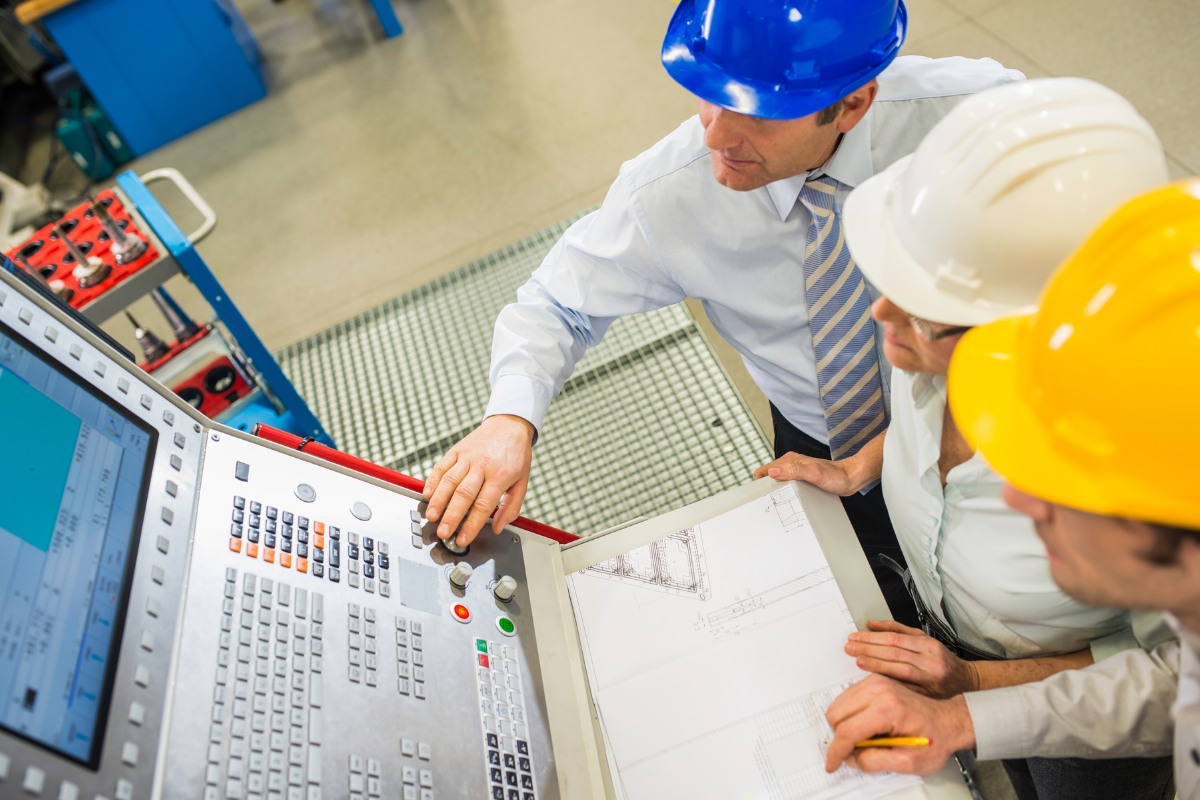
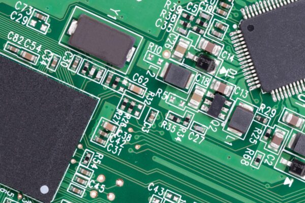
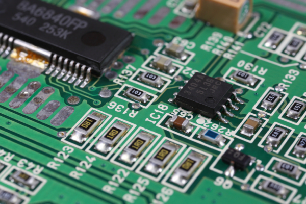
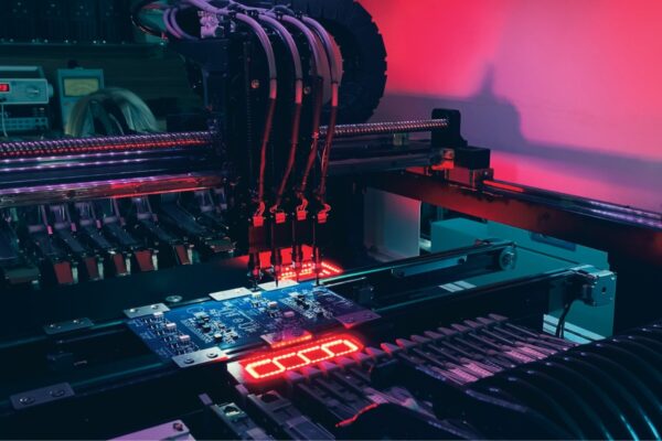
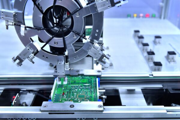
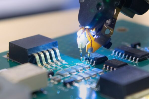
CAM data and job-specific information are received from our customers and carefully checked by CAM room personnel for completeness. The board pattern is copied and arranged to utilize a panel that will be used throughout the manufacturing process. Tooling holes, test coupons, and identity information are then added to the layout. The data is converted into formats used throughout the manufacturing process in equipment such as the laser photoplotter, CNC drilling and routing machines, AOI, and electrical testers. The work of the CAM department is greatly enhanced by the quality of the data package supplied by the customer. Typical shortcomings of the customer’s data include poorly dimensioned or lack of drawings, no read-me text file, poor or non-existent notes or specifications, and designs not created using design standards (i.e., non-IPC).
Film Room
Under controlled environmental conditions, a set of master film tools are plotted using our fully automatic laser photoplotters and film processing equipment. The master film tools are then inspected and copied to diazo film for use by the imaging, screening, and inspection personnel.
Inner-Layer Processing
The imaging personnel start by laminating a copper-clad core (inner layer) material with a photosensitive etch resist film. Silver film tools are registered on the laminated cores and exposed with an ultraviolet light source. The inner layer is then developed, removing the resist film from the copper in the areas that will eventually become free of copper. The exposed copper is then removed using an etching solution that dissolves the copper. Finally, the etch resist film is removed, revealing the finished inner layer panel.
Multilayer Lamination
In the lamination area, the finished inner layer panels are treated in a process that produces a dark brown/black surface on the inner layer. This modified surface increases the adhesion of the multilayer board. The prepared inner layers are stacked alternately with a partially cured epoxy sheet material called prepreg to create the multilayer panel. The panels are then placed in a hydraulic press and pressed under extreme pressure and heated for a predetermined amount of time. The prepreg material melts and is forced into the spaces between the interlayer conductors. When the molten epoxy reaches the exact temperature, it solidifies, at which time the epoxy finishes curing. When the cycle has ended, the panels are cooled and removed from the press, now ready for the drilling operation.
Drilling
The base materials from the suppliers or pressed multilayer panels are stacked up on our multi-spindle CNC drilling equipment. Solid carbide drill bits are loaded into magazines and placed into the drilling machine. The program created in the CAM room is loaded into the controller, and the program runs. The drilling operation is fully automatic from there. The machine loads the drill bits into high-speed air bearing spindles, sets the speeds and feed rates, and checks drill diameter, length, and run-out.
Hole Activation
The hole activation is a process involving a series of chemical solutions that clean, prepare, and activate the hole walls with copper, producing an electrically conductive hole. This will allow copper to electroplate to the epoxy core material, creating a plated through hole. This is the start of the electrical interconnection of the internal and outer layers.
Imaging
A photosensitive resist film is laminated to the drilled panel. Diazo film tools are registered to the laminated panels and then exposed to an ultraviolet light source. The photoresist is developed, revealing the copper in the areas that will eventually remain as conductors.
Plating / Etching
The imaged panels are then chemically cleaned and loaded into an electroplating tank. Copper is electroplated onto the hole walls and to the exposed conductor areas. Metal will not plate to areas masked by the photoresist film. The panels are transferred to a tin electroplating tank for a thin layer of tin plating. This tin layer is used to protect the newly plated copper from the etching process. The resist film is removed, revealing the copper areas to be etched. The unwanted copper is dissolved using an etching solution, leaving only the areas protected by the tin plating. The tin is then removed, revealing copper conductors and land areas.
Masking
The plated and etched panels are cleaned and inspected prior to the application of the solder mask coating. The solder mask coating is then applied in a conveyorized spray machine followed by an IR tack dry. The solder mask used is called LPI (liquid photo-imageable) and is light-sensitive. After tack drying, a diazo film tool is registered to the coated panel, and the panel is exposed to an ultraviolet light source. The solder mask coated panel is then developed, which removes the mask and exposes the pads or any areas protected by the film tool. Lastly, the panels are baked to finish curing the solder mask ink.
Surface Finishing
Panels can then be sent through several different processes to produce a variety of surface finishes. The most common of which is the hot air solder leveling (HASL) process. In this process, the panel is chemically cleaned, and flux is applied.
Other surface finishes include electroplated gold (Au) over nickel (Ni), electroless nickel immersion gold (ENIG), white tin, and a lead-free solder finish. For lead-free finishes that meet the RoHS directive, ENIG, white tin, and lead-free solder are offered.
Marking / Legend
All of the silkscreen marking and legends applied at Vista Technology are done using an LPI (liquid photoimageable) ink. This ensures the very sharpest of images for not only very small features (<.006″) but also for features that are placed over high-profile circuitry.
Routing
Finished panels are profiled or cut out using a CNC router. The router is programmed to create the dimensional profile of the individual board. Using carbide cutting bits, the machine routs the profile of the board. The dimensions of the finished board are checked to print. The boards are then cleaned and sent to our testing and inspection areas.
Testing and Final Inspection
Data from the customer is converted to the necessary format required by our testing equipment. The test data created will test the finished board to the customer’s supplied design. Individual boards are loaded onto the tester, and the machine runs a sequence of electrical tests. Boards passing the electrical tests for both isolation and resistance are marked and sent to our final inspection department.
Quality Control
Quality control is an integral part of the entire CAM process. Each stage of production is meticulously monitored to ensure that the final product meets the highest standards. This includes regular inspections, testing, and validation to catch any discrepancies early on. By maintaining stringent quality control measures, we ensure that the final product is reliable and meets customer specifications.
Environmental Considerations
In today’s manufacturing landscape, environmental considerations are more important than ever. Our CAM processes are designed to minimize waste and reduce environmental impact. This includes using eco-friendly materials, recycling waste products, and ensuring that all chemical processes are compliant with environmental regulations. By prioritizing sustainability, we not only meet regulatory requirements but also contribute to a healthier planet.
