In the intricate world of electronics manufacturing, ensuring the quality and reliability of Printed Circuit Board Assemblies (PCBAs) is paramount. This is where Automated Test Equipment (ATE) plays a vital role. This article provides a comprehensive overview of ATE in PCBA testing, delving into its fundamentals, various types, working principles, benefits, and advanced techniques. Whether you’re new to the field or a seasoned researcher, this guide will equip you with a thorough understanding of this critical aspect of electronics manufacturing.
What is Automated Test Equipment (ATE)
Automated Test Equipment, commonly known as ATE, is a sophisticated system designed to automatically test electronic devices, including PCBAs, for functional and parametric defects. Imagine a highly efficient and precise robotic inspector that meticulously examines each component and connection on a circuit board. That’s essentially what ATE does. These systems employ software-controlled instrumentation to apply specific stimuli to the device under test (DUT) and measure its responses.
The measured responses are then compared against expected values, allowing the system to quickly determine if the DUT is functioning correctly. This automated process significantly reduces testing time compared to manual methods and dramatically improves test accuracy and repeatability. In essence, ATE plays a crucial role in ensuring the quality and reliability of the electronic products we rely on daily, from smartphones to medical devices. It acts as a gatekeeper, preventing faulty products from reaching the market and ensuring that only high-quality electronics make their way into our hands.
Types of ATE for PCBA
Several types of ATE systems are used in PCBA testing, each with its strengths and weaknesses. Let’s explore some of the most common ones:
In-Circuit Testers (ICT)
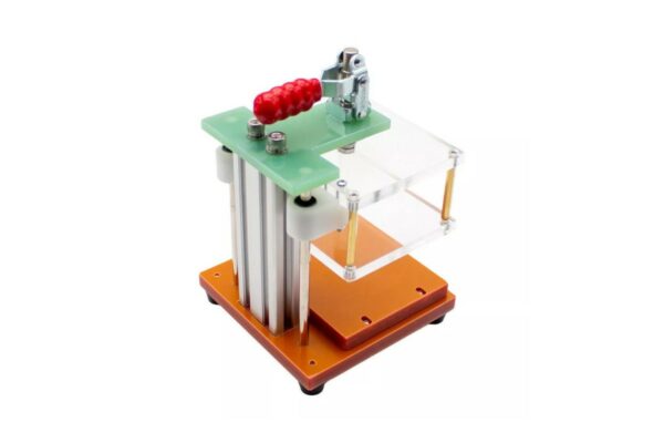
In-Circuit Testers, or ICTs, are like meticulous detectives, examining each component on a PCBA individually after soldering. They use a specialized fixture known as a “bed of nails” – a platform with spring-loaded pins that make contact with specific test points on the board. ICTs can measure the value of resistors, capacitors, inductors, and other components, ensuring they are within specified tolerances. They can also detect common manufacturing defects like shorts, opens, and incorrect component placement.
Think of it like testing each light bulb in a string of Christmas lights individually to make sure they are all working correctly. While highly effective for identifying manufacturing defects, ICTs have limitations. They cannot test the overall functionality of the entire circuit, and they may require a large number of test points, which can be challenging for densely packed boards.
Flying Probe Testers
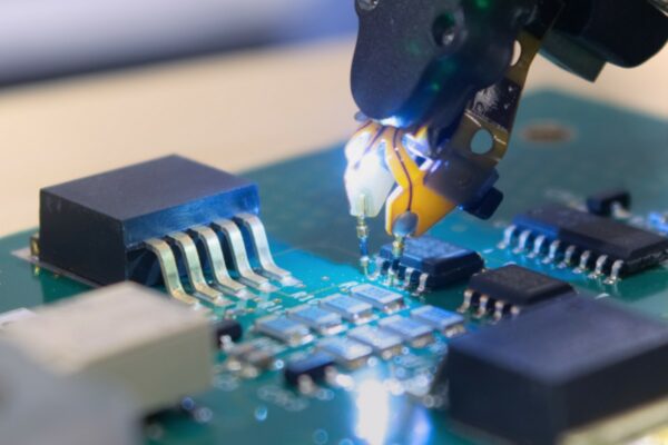
Flying probe testers offer a more flexible approach to PCBA testing. Unlike ICTs, they don’t rely on a fixed “bed of nails.” Instead, they use two or more probes that move around the PCBA, making contact with test points as needed. This agility makes them ideal for low-volume production and prototype testing, as they don’t require a dedicated fixture for each board type.
Flying probe testers can perform similar tests as ICTs, such as measuring component values and detecting shorts and opens. However, they are generally slower than ICTs. The trade-off is flexibility for speed. They are particularly useful when dealing with frequent design changes, as reprogramming the tester is much easier than creating a new fixture.
Functional Circuit Testers (FCT)
Functional Circuit Testers, or FCTs, take a holistic approach to testing. Instead of examining individual components, they assess the overall functionality of the assembled PCBA. FCTs simulate the board’s actual operating environment, applying functional inputs and measuring the outputs to verify that it performs as intended.
For example, if the PCBA is designed for a digital clock, the FCT would simulate the signals that the clock would receive in its final application and check if the outputs (e.g., display, timekeeping) are correct. This type of testing can detect defects that ICTs might miss, such as timing issues and functional failures that only become apparent when the entire circuit is operating. FCTs are often used as a final “seal of approval” before a product is shipped.
Burn-In Testing Systems
Burn-in testing is a crucial process for identifying early-life failures in PCBAs. It’s like a stress test for electronics, pushing them to their limits to weed out any weak components. Burn-in systems typically consist of an oven or chamber that maintains a controlled, elevated temperature. The boards are powered on and subjected to functional tests during this “burn-in” period.
This process helps to accelerate the aging of components, causing those with latent defects to fail early on. By identifying and eliminating these weak components, burn-in testing significantly improves the long-term reliability of electronic products. The duration and temperature of the burn-in process are carefully determined based on product requirements and industry standards.
Automated Optical Inspection (AOI)
Automated Optical Inspection, or AOI, systems are the “eyes” of the ATE world. They use cameras and sophisticated image processing software to visually inspect PCBAs for defects. AOI systems can quickly detect issues such as missing components, incorrect component orientation, solder bridges, and insufficient solder.
Think of it as a high-speed visual quality check that can spot even the tiniest imperfections. AOI is often used as a first-pass inspection to identify gross manufacturing defects, providing a quick and efficient way to catch obvious problems. Advanced AOI systems can even perform 3D inspections, measuring component height and solder joint volume to provide a more comprehensive assessment.
X-Ray Inspection Systems
X-ray inspection systems take us into the hidden world beneath the surface of a PCBA. They use X-rays to create images of the internal structure of the board, revealing defects that are invisible to the naked eye. This is particularly useful for inspecting Ball Grid Array (BGA) packages and other components with hidden solder connections.
X-ray inspection can detect issues such as voids in solder joints, internal shorts, and misaligned components. Both 2D and 3D X-ray systems are available, with 3D systems providing a more detailed and comprehensive view of the internal structure, allowing for a more thorough analysis.
Key Components of ATE Systems
ATE systems are complex machines composed of several key components working together seamlessly:
- Test Instrumentation: This is the heart of the ATE system, providing the tools needed to test the PCBA. It includes power supplies to energize the board, signal generators to create test signals, digital multimeters (DMMs) to measure voltage and current, oscilloscopes to analyze waveforms, and other specialized instruments.
- Switching Systems: These act as the traffic controllers of the ATE system, routing signals between the test instrumentation and the various test points on the DUT. They allow multiple test points to be connected to a limited number of instruments, optimizing resource utilization.
- Test Fixtures: These provide the physical interface between the ATE system and the DUT. For ICT, this is the “bed of nails” fixture, while functional testers may use edge connectors or custom cables to connect to the board.
- Software and Programming: The brains of the ATE system. This software defines the test sequence, controls instrument settings, and sets the pass/fail criteria. Test programs are often written in languages like C++, Python, or specialized test languages.
How ATE Works in PCBA Testing
The process of testing PCBAs using ATE involves several key steps:
Test Program Development
Creating a test program is the first crucial step. Test engineers develop these programs based on the PCBA’s design specifications and test requirements. The program defines the precise sequence of tests, the stimuli to be applied, and the expected responses from a healthy board. This requires a deep understanding of both the PCBA’s functionality and the capabilities of the ATE system. Often, these programs also include diagnostic routines to pinpoint the root cause of any failures detected.
Fixture Design and Fabrication
The test fixture is a critical component that provides a reliable electrical connection between the ATE system and the DUT. For ICT, this involves designing a “bed of nails” fixture with spring-loaded probes (pogo pins) precisely positioned to contact specific test points on the PCBA. Functional test fixtures might use edge connectors, custom cables, or a combination of methods. Fixture design requires careful consideration of probe placement, signal integrity, and mechanical stability. These fixtures are typically fabricated using precision machining and assembly techniques to ensure accuracy and durability.
Test Execution, Data Analysis, and Interpretation
Once the PCBA is placed in the test fixture, the test program is executed. The ATE system springs into action, applying the specified stimuli and meticulously measuring the responses. This data is then compared against the expected values defined in the test program. Test results are displayed to the operator, clearly indicating whether the board passed or failed. But the process doesn’t end there.
Data Analysis
ATE systems are data powerhouses, collecting vast amounts of information during testing. This data is a goldmine for identifying trends, patterns, and potential process improvements. Statistical Process Control (SPC) techniques are often employed to monitor test results, detecting any deviations from expected performance. When failures occur, detailed failure analysis is performed to uncover the root cause of defects.
Data Interpretation and Actionable Insights
Interpreting ATE data requires a blend of expertise in both the testing process and the PCBA’s functionality. Test engineers delve into failure logs, parametric measurements, and other data points to identify the specific components or processes causing defects.
For instance, if a particular component consistently fails a solder joint test, it might indicate a need to adjust the reflow soldering profile or improve the component’s solderability. This valuable information can be used to refine the manufacturing process, optimize designs, and ultimately enhance product quality.
Let’s take a deeper dive into how we might use advanced statistical methods to analyze ATE data. One powerful technique is Pareto analysis, which helps identify the most significant defect types. By plotting the frequency of different defect types on a Pareto chart, we can quickly see which issues are causing the most problems. For example, we might find that 80% of our defects are due to solder bridges and missing components. This allows us to focus our improvement efforts on these critical areas.
Another valuable tool is the Weibull distribution, which is particularly useful for analyzing reliability data from burn-in testing. The Weibull distribution can help us model the time-to-failure of components and predict the long-term reliability of our products. By analyzing the shape and scale parameters of the Weibull distribution, we can gain insights into the dominant failure mechanisms and optimize our burn-in process accordingly.
Benefits of Using ATE in PCBA Testing
The advantages of using ATE in PCBA testing are numerous:
- Increased Test Throughput: ATE systems can test PCBAs much faster than manual testing, significantly boosting production output.
- Improved Test Coverage: ATE can perform a wider range of tests compared to manual methods, ensuring that more potential defects are detected.
- Enhanced Accuracy and Repeatability: ATE systems deliver consistent and accurate test results, eliminating the risk of human error.
- Reduced Labor Costs: Automation reduces the need for manual testing, leading to significant labor cost savings.
- Data Logging and Traceability: ATE systems automatically log test results, providing valuable data for process improvement and ensuring traceability.
Understanding Test Coverage in ATE
Test coverage is a critical concept in ATE. It refers to the extent to which a PCBA is tested for potential defects, often expressed as a percentage of the total possible faults that can be detected. High test coverage is essential for ensuring product quality and reliability. But how do we achieve it?
Fault Spectrum Analysis
This is a method for identifying the types of faults that are likely to occur in a PCBA. It involves a thorough analysis of the manufacturing process, component types, and design characteristics to determine potential failure mechanisms. Common fault types include shorts, opens, wrong component values, missing components, and functional failures. Understanding the fault spectrum helps in selecting the appropriate ATE techniques and optimizing test coverage.
Test Point Selection Strategies
Test points are specific locations on the PCBA where electrical measurements can be made. Selecting the right test points is crucial for achieving high test coverage. Strategies aim to maximize fault detection while minimizing the number of test points used. Factors to consider include component accessibility, signal integrity, and the capabilities of the ATE system. Design for Testability (DFT) guidelines often recommend placing test points on all critical nets and component pins to ensure thorough testing.
Advanced ATE Techniques for Complex PCBAs
As PCBAs become increasingly complex, advanced testing techniques are needed to ensure their quality and reliability.
Boundary Scan Testing
Boundary scan, also known as IEEE 1149.1 or JTAG, is a powerful method for testing interconnections between integrated circuits (ICs) on a PCBA. It uses special test logic embedded within the ICs to control and observe the signals at their pins. This allows for the detection of shorts, opens, and other defects in the connections between ICs, even when physical access to test points is limited. Boundary scan is particularly useful for testing complex, high-density PCBAs, and it can be integrated with other ATE techniques to provide comprehensive test coverage.
Built-In Self-Test (BIST)
BIST is a technique where a PCBA or IC is designed to test itself. Special circuitry is added that generates test patterns and analyzes the responses, allowing the device to check its own functionality. BIST can be used to test digital circuits, memory devices, and other components. It can reduce the need for external ATE, especially for in-field testing and diagnostics. BIST can also be combined with ATE to improve test efficiency and reduce test time.
System-Level Testing
System-level testing involves testing the PCBA as part of a larger system. This verifies that the PCBA interacts correctly with other components and performs its intended function within the overall system. System-level testing can detect integration issues and functional failures that might not be caught by lower-level tests. It often requires specialized test equipment and software that can simulate the system environment realistically.
Signal Integrity, Power Integrity, and Thermal Testing
These specialized tests address critical aspects of modern PCBA performance.
Signal Integrity Testing
This ensures that signals propagate correctly across the PCBA without excessive distortion, reflection, or crosstalk. It involves measuring parameters such as impedance, rise time, and eye diagrams. Specialized ATE equipment, such as Time Domain Reflectometers (TDRs) and Vector Network Analyzers (VNAs), are used. Signal integrity is crucial for high-speed digital and RF circuits.
Power Integrity Testing
This verifies that the power distribution network (PDN) on the PCBA provides clean and stable power to all components. It involves measuring parameters such as DC voltage drop, AC ripple, and transient response. Specialized probes and instrumentation are used to analyze power integrity. This is vital for preventing power-related failures and ensuring reliable operation.
Thermal Testing
This assesses the thermal performance of the PCBA under operating conditions. It involves measuring the temperature of components and the PCB using thermal cameras or sensors. Thermal testing can be combined with burn-in testing to identify thermal hotspots and potential reliability issues. It helps to optimize the thermal design of the PCBA and prevent overheating, which can lead to premature failures.
Choosing the Right ATE for PCBA Testing
Selecting the appropriate ATE system is a critical decision that can significantly impact the efficiency and effectiveness of PCBA testing.
Factors to Consider
Several factors must be considered when choosing an ATE system:
PCBA Complexity
The complexity of the PCBA, including component density, signal speeds, and the presence of analog or mixed-signal circuits, will influence the choice of ATE. More complex boards may require more sophisticated testing capabilities.
Production Volume
High-volume production typically justifies the higher cost of ICT systems, which offer faster testing speeds. Low-volume production may be better suited for more flexible but slower flying probe testers.
Test Requirements
The specific types of tests required (e.g., in-circuit, functional, boundary scan) will determine the necessary ATE capabilities.
Budget
The initial cost of the ATE system, as well as ongoing programming and maintenance costs, must be carefully considered.
Flexibility
The ability of the ATE system to adapt to design changes and test new products is an important factor, especially in rapidly evolving industries.
Comparing Different ATE Types
When comparing different ATE types, it’s essential to weigh their strengths and weaknesses:
ICT vs. Flying Probe
ICT offers higher throughput but requires dedicated fixtures for each board type. Flying probe is more flexible and adaptable to design changes but is slower.
ICT vs. FCT
ICT focuses on testing individual components, while FCT tests the overall functionality of the board.
AOI vs. X-ray
AOI detects visual defects on the surface of the board, while X-ray can detect hidden defects beneath the surface.
Often, the optimal choice involves a combination of different ATE types to achieve comprehensive test coverage. For example, a manufacturer might use AOI for initial screening, followed by ICT for component-level testing, and finally FCT for functional verification.
Cost Analysis and Return on Investment (ROI)
A thorough cost analysis is essential when investing in ATE.
Initial Investment
This includes the cost of the ATE system itself, along with any necessary fixtures and software.
Programming Costs
This encompasses the cost of developing and maintaining test programs, which can vary depending on the complexity of the PCBA and the ATE system.
Maintenance Costs
This includes regular calibration, repairs, and the cost of spare parts to keep the ATE system running smoothly.
Labor Savings
Automation reduces the need for manual testing, resulting in significant labor cost savings over time.
Yield Improvement
By detecting defects early in the manufacturing process, ATE can significantly improve product yield, reducing scrap and rework costs.
ROI Calculation
ROI is calculated by dividing the net benefits (cost savings and yield improvement) by the total cost of ownership (TCO). TCO includes all costs associated with the ATE system over its lifetime, including initial investment, programming, and maintenance. A positive ROI indicates that the ATE investment is financially beneficial.
Let’s delve deeper into calculating ROI. Here’s a step-by-step guide:
- Estimate the annual cost of defects without ATE: This includes the cost of scrap, rework, and potential field failures. You can estimate this based on historical data or industry benchmarks.
- Estimate the annual cost of defects with ATE: This should be significantly lower than the cost without ATE, as ATE helps catch defects early.
- Calculate the annual cost savings: Subtract the estimated cost of defects with ATE from the cost without ATE.
- Estimate the annual labor savings: Calculate the difference in labor costs between manual testing and automated testing.
- Calculate the total annual benefits: Add the annual cost savings and annual labor savings.
- Estimate the total cost of ownership (TCO) of the ATE system: This includes the initial investment, annual programming costs, and annual maintenance costs, projected over the expected lifespan of the ATE system.
- Calculate the net benefits: Subtract the TCO from the total annual benefits multiplied by the lifespan of the ATE system.
- Calculate the ROI: Divide the net benefits by the TCO.
For example, let’s say a company estimates that without ATE, they incur $500,000 annually in defect-related costs. With ATE, they project this cost to drop to $100,000, resulting in $400,000 in annual cost savings. They also estimate $100,000 in annual labor savings. The total annual benefits would be $500,000.
If the TCO of the ATE system over its five-year lifespan is $1,000,000, the net benefits would be ($500,000 * 5) – $1,000,000 = $1,500,000. The ROI would be $1,500,000 / $1,000,000 = 1.5, or 150%. This indicates a strong return on investment.
Balancing Test Coverage and Cost
Now, let’s discuss the crucial aspect of balancing test coverage and cost. It’s not always feasible or cost-effective to test for every single possible defect. We need a strategic approach to optimize this balance. Here’s a decision-making model:
- Risk Assessment: Identify the most critical components and functions of the PCBA. Consider the potential impact of failures in these areas on product performance, safety, and customer satisfaction.
- Prioritize Tests: Based on the risk assessment, prioritize tests that address the most critical areas. Focus on tests that have the highest probability of detecting defects that could lead to significant consequences.
- Cost-Benefit Analysis: For each test, evaluate its cost (programming, fixture, test time) against its potential benefits (defect detection, improved yield, reduced field failures).
- Defect Escape Rate: Estimate the likelihood of defects escaping detection for different test strategies. Consider the cost of field failures and weigh it against the cost of additional testing.
- Iterative Optimization: Continuously monitor test results, analyze defect escape rates, and refine the test strategy to optimize the balance between test coverage and cost.
For instance, a medical device manufacturer might prioritize tests for components involved in critical life-support functions, even if these tests are more expensive. They might accept a slightly higher defect escape rate for less critical functions to keep overall testing costs within budget.
